Saras Micro Devices has developed technology to embed capacitors and inductors into semiconductor substrates and PCB laminates. Doing so keeps them close to loads through vertical power delivery,
Every day, we hear about the need for more power to satisfy AI chips. The combination of low voltage and high current (1000s of amps) means that any electrical path, even short paths, results in unacceptable power losses. Moving voltage regulations and their associated passive components closer to the load reduces those losses.
Vertical power delivery (VPD), a design concept that places power components on the underside of PCBs rather than alongside loads, reduces losses. What if you could place passive components such as capacitors and inductors inside PCBs or even inside module substrates? That could further reduce losses. Saras Micro Devices has developed technology to do that. How do they do it? To find out, EE World spoke with Eelco Bergman, Chief Business Officer. In the video and the edited transcript that follows, Bergman explains how the components are constructed and how they get embedded into substrates and laminates.
Saras Micro Devices has developed a technology where they build capacitors and inductors that can then be embedded directly into PCB material, into voltage-regulator modules, the loads themselves, anywhere in that path. To learn how that technology works and how it’s used, we spoke with Eelco Bergman of Saras Micro.
EE World: Eelco, please start by telling EE World a little bit about Saras Micro Devices, how it got started, and then we’re going to talk about your technology for use with power delivery.
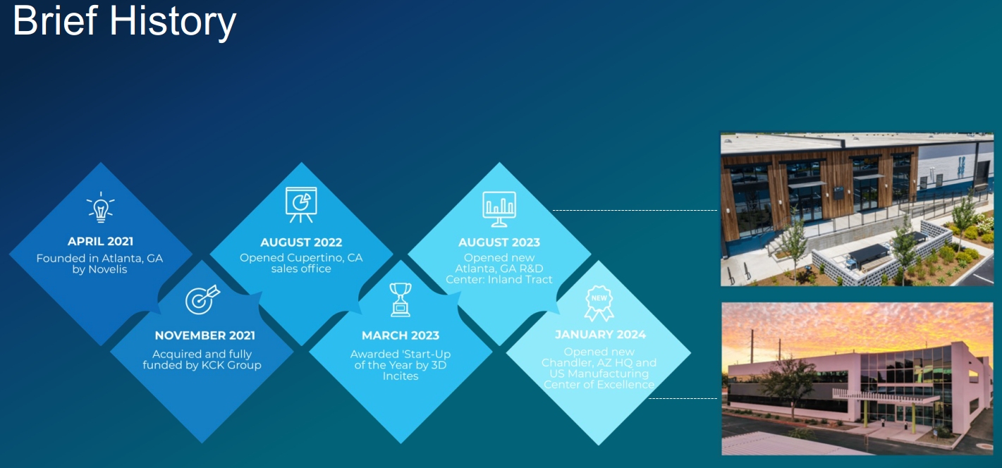
Bergman: The company was started as a research and development project inside an aluminum materials company based in Atlanta, named Novelis. They were having the team look at how aluminum materials could be utilized for electronic industry purposes.
The team came up with a way to leverage modified aluminum materials to make capacitors. Once that had been established, Novelis spun Saras out as an independent company, and that was in April of 2021. Later that year, they sold the company to our current investor, KCK group. That was late 2021. In 2022, the KCK team spent the better part of that year building out a new leadership team, which included myself, as well as our current CEO, COO, and CTO. We were all in place by the start of 2023, at which point we took the technology that was available and defined a product to bring to market.
In August of 2023, Saras opened a new R&D Center in Atlanta. We’ve been operating out of a small incubator space. Today, we have a team of 20 to 25 people in Atlanta developing our capacitor and inductor technology. In January 2024, we opened a facility in Chandler, Arizona, where we are establishing and installing our initial volume-manufacturing capability.
EE World: Where does management come from?
Bergman:Our leadership team comes heavily from the packaging industry. Since the company’s focus was really about how we can leverage this aluminum capacitor technology to help power-delivery challenges faced by the AI industry.
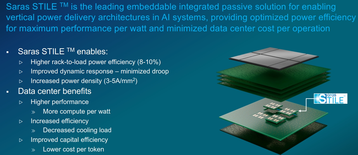
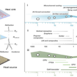
AI is more than just the next killer app. This is really an infrastructural change that will dramatically alter the way many industries operate. There’s a trend toward gigawatt scale, mega campuses for these data centers. With that comes data center rack power, as well as going to increasingly higher densities, where moving from 8 kW to 12 kW or 20 kW per rack, going as high as a megawatt per rack. This means more power required in small spaces.
We’ve all heard about the strain that this power demand is putting on the infrastructure and its ability to deliver that power for data center operators and the device makers that supply them. The question is, how do you make sure you’re making the most efficient use possible out of the power that is available to you to maximize your performance per watt, minimize your cost per operation, and minimize your cost per token? There’s a huge focus now on what do we do to improve efficiency.
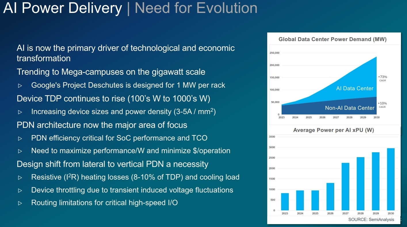
You see these xPUs use going from hundreds to thousands of watts. We’re now talking about 1.5 kW and above per device given the amount of silicon that’s being integrated into one of these single packages.
These advanced processor engines are no longer just one chip. They’re a set of multiple devices, including HBM (high-bandwidth memory), GPUs, and other types of chiplet devices. The voltages continue to drop, so power delivery efficiency is really key.
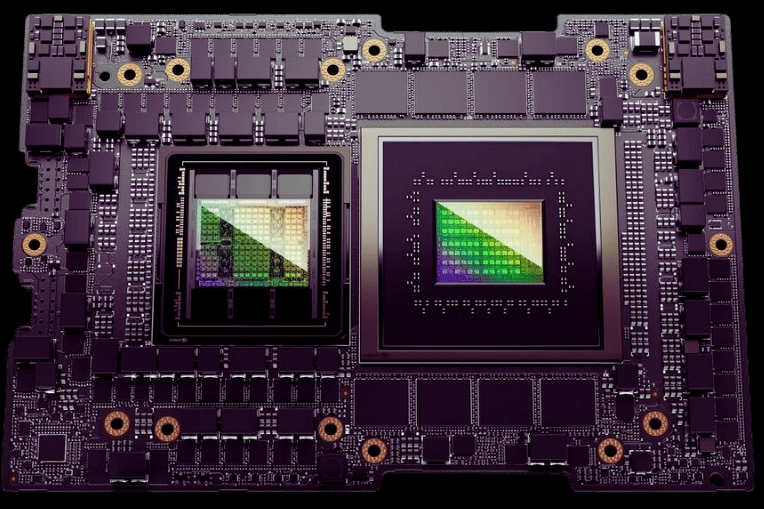
If you look at a typical AI board, such as this Nvidia H200 board, everything that’s associated with power conversion sit up on top of the board, and this is called lateral power delivery. But, as the power goes up, the space becomes limited for these components. Also, the power-delivery components are impacting the ability to route critical AI signals. So this is where a real change needs to be made in how power is delivered.
EE World: Why does mounting power components on the same side of the board as the GPU cause problems?
Bergman: When you have power delivered laterally, you have a lot of resistive losses in the board for very high amounts of current that are going into the chip. These losses are a function of the square of the current times the resistance (I²R). As the power levels keep going up, the amount of power lost due to resistive losses becomes ever more impactful, and it has a secondary impact of generating a lot of heat, which means you have to spend more power and money on cooling.
The industry is moving to vertical power delivery, which moves at least a portion of that power delivery from lateral to vertical underneath the device, thereby shortening the power delivery path and reducing those resistive losses.
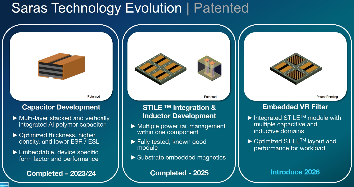
At Saras, we’ve developed this aluminum-based capacitor made from a modified aluminum foil. It provides very high surface area and provides a high-density capacitive material in a single layer that’s 130 to 150 microns thick. We can stack up multiple capacitors into a single component. By doing so, we multiply the capacitive density of the part, which reduces the resistance. When you connect these capacitors in parallel, you get lower resistance. So what you see is this capacitive element is kind of the base building block.

We can configure these capacitors to different X–Y sizes. By adding and subtracting layers, make them thicker or thinner, but our objective in making these is that, because they have these copper terminations, and they essentially pass through from top to bottom, it makes it very easy to embed these components into the core of the IC package substrate or into a PCB, giving you access to both anode and cathode on both sides of that board.
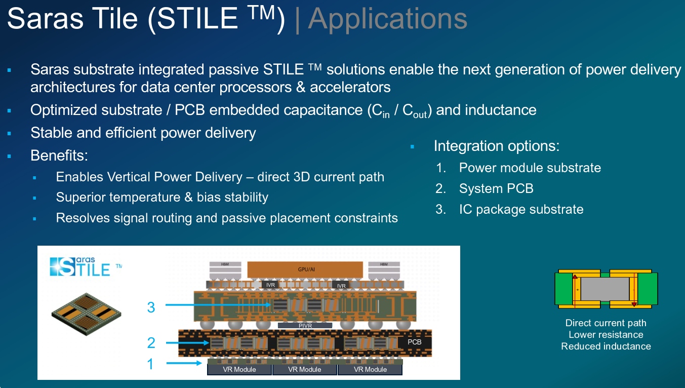
Then the next thing we’ve done is we work with the customers such as SoC suppliers and power-module suppliers. We say, “How much capacitance do you need where?” We pre-embed them into what we call our Saras tile. And these tiles can be completely custom configured based on the customer requirements.
We try to stick with standard capacitive elements, and later, also inductive elements, and then we configure them into custom modules for the customers. These modules are then what gets embedded into the substrate or the PCB, so it helps reduce the risk for the substrate manufacturer and makes it easier for them to embed known-good components.
Here, you see an example of a package substrate. You have the substrate core, which is typically anywhere from 0.8 mm to 1.6 mm thick. You see our tiles. In this case, it’s a 2×2 array of capacitors in each tile. Those would get embedded in the core, and then the substrate maker does their build-up layer fabrication on the top and bottom of that core, the same way they do today. By doing that, we’re enabling vertical power delivery, because now we’re directly between the power conversion module and the load, which is the xPU engine sitting up on the top. Our tiles can have multiple insertion points.
EE World: Where do these tiles go?
Bergman: Initially, they probably will go on the output side of these VR modules, which are being moved from the top of the PCB to the bottom. Then they could go from being buried inside those module substrates, and go inside the PCB. As customers continue to disaggregate their power-delivery network and start using IVR devices or packaged IVRs, which do a lower voltage conversion, maybe from 2 V or 3 V to the point of load, then we can support the output side by embedding ourselves into the package substrate.
EE World: If I were to look at this as a schematic, would these capacitors function as bypass or decoupling capacitors? That is the intent of putting these capacitors there to get them as close to the VR module and the load as possible? Is that correct?
Bergman: Yes, although if you’re talking about I/O decoupling right at the chip level, these capacitors don’t operate like that. They’re not that small, and they don’t operate at those frequencies. For example, if you’ve got a buck converter on the bottom, going from 12 V to point-of-load, or from 12 V to 2 V or 3 V, the output side of that needs to be filtered, and that’s where our capacitors play a role. So you’re typically dealing with lower frequencies today, it might be 2 MHz to 3 MHz. It’s going to 5 MHz and maybe even as high as 10 MHz.
As you move closer to the die, particularly if you then have an IVR that’s doing a step from, say, 2 V to point-of-load right under the die, then your frequencies do get much higher, and the amount of capacitance you need decreases commensurately. The same would be true for the inductor.
EE World: So if these capacitors and inductors decrease in size with frequency, is there a point where manufacturing them becomes more difficult or expensive just because they’re smaller? And that leads me to also wonder, how do you actually manufacture these? How do you put that all together?
Bergman: As you get closer and closer and you need lower value, smaller, passive components that operate at higher frequency, that is actually served by a different set of solutions today. So if you look at deep-trench capacitors that are being put into silicon interposers or into fan-out interposers, those are the components that are handling that near-die portion of the decoupling and filtering. But there are multiple stages to these power conversions because you’re still coming in from the rack at 48 V to 54 V. Now people are even talking about higher voltages for the rack bus. So, you need multiple steps to step down, and we’re playing more in those initial step-downs, rather than that final step-down to the point of load.
I’m not going to go into a lot of detail on how we make our caps, but we source the incoming materials from external partners. Our capacitor process includes steps to take this very high surface area, aluminum material and turn it into a capacitor. As I mentioned, we integrate and stack those up and connect them in parallel, and that’s really leveraging packaging technology into those tiles, and that is exactly what we’re setting up in our facility in Arizona. As a matter of fact, all the tools are in place. We’re now qualifying the internal processes.
EE World: So let me make sure I understand how these capacitors and inductors get embedded, because I’m looking at the figure in the slide and you show three options. Would you supply these capacitors, for example, to a PCB manufacturer? They then embed these capacitors into the board? Who does that?
Bergman: So we do the initial embedding of the capacitors and the inductive elements, the standard elements, into the tile. The tile could be 10 mm × 10 mm. Could be 5 mm × 8 mm, whatever the customer needs. We position the capacitive and inductive domains where the customer needs them. Then we ship those tiles to the substrate supplier or the PCB supplier, and the tiles will already be designed to match their layer or core thicknesses.
If you think about an IC package substrate, the first step in making a package IC substrate is you take a panel of copper clad laminate from Resonac or someone like that, and they drill all the mechanical through vias that need to go through that core layer, because that layer is thick. It might be like I said, 800 (0.8 mm), 1.2 mm, 1.6 mm thick.
At that time, the substrate supplier would also route a cavity, and you would drop the tile into that cavity. It’s a through cavity, all the way top-to-bottom. You would drop the tile in, fill around the edge, and then planarize both sides. And then they would start to do their build up, film type additive layer. So here’s the core image layer, which is that single-layer copper-clad laminate, and these tiles get embedded in that layer, and then you start to do your build-up layers, which then connect to the capacitors from both sides.
But you have essentially a through contact top to bottom, whereas if you embed an MLCC (multilayer ceramic capacitor) or a silicon DTC (digitally tunable capacitor), those have only connections on one side, or they’re because they’re so deep in the cavity, the connections only on one side, so you have to actually route around them to get to the other side. So we avoid that, and that helps reduce the inductive loop as well as save space.
EE World: Is there any issue with heating problems that have to be addressed?
Bergman: Absolutely. Thermal is a big consideration when you’re looking at this vertical power delivery. And it really starts with the VR and then the components that support them, whether it be inductors or capacitors. So that is, without question, a key factor, and that becomes a limitation on how much power conversion you can do at each stage.
Going along with that is you’re significantly improving the efficiency of your power-delivery path. So your heat generation is also going down, and it’s just finding that optimum of how much can I do to avoid adding too much heat, and how much efficiency am I gaining that’s helping me reduce that heat?
But what you see in a lot of these vertical power applications where SoC providers are looking at putting the power conversion underneath their OAM (OCP Accelerator Module) card or on the backside of their PCIe card, is that they are leaving space to actually be able to insert a cool plate between the back of those power conversion modules and the underlying server motherboard. Because what you don’t want to do is you don’t want to add more thermal to the xPU itself, because now you’re taking away performance.
EE World: You recently attended DeisnCon and APEC. Why do you see DesignCon as an attractive place to show this technology?Bergman: Years ago, DesignCon was very much focused on the chip design and all the IP and other factors around it. The reality is today that to continue to evolve with Moore’s Law slowing, other techniques are being used to achieve continued increased performance, lower latency, higher bandwidth, and that those other solutions are how do we take the components that have traditionally lived adjacent to our devices on our system board and bring them closer and closer together, and thus you get this heterogeneous integration and the adoption of chiplets.
All of that is enabled by packaging. It’s the continued miniaturization of a system into a package. So these are really the ultimate system-in-package type solutions, where you’re just taking what’s historically been interconnected on a PCB board and bringing it closer and closer together. By doing that, the power densities, the total power required, continues to increase, with the latency requirements, the operating frequencies are going up. The integration of power is really the next step.
And what we’ve seen over the last several years at DesignCon is that there’s an increasing amount of focus on packaging technology and how it enables these advanced chip designs, but also very specifically on how does power, what is the power delivery network architecture look like to support these ever rising levels of power density and total power required to operate these heterogeneously integrated devices?
So for us, it’s become increasingly more interesting to be present, to be able to show how our solution can help enable some of these advanced topologies that are being considered for power delivery, and the people we’re reaching out to are both the SoC developers and suppliers, because they’re thinking about it from a fully integrated package level, as well as the system PCB designers and the power module providers, who have to integrate their solutions into these high density packages. Our goal is to continue to get that message out to the people who will ultimately benefit from this, which ranges from the SoC maker to the data center operator.
EE World: Eelco, thank you very much for your time. This was very interesting. I had never seen this kind of technology before, and it’s always interesting to learn something new. So thank you for taking the time to speak with us at EE World.
Bergman: Martin, thank you very much. We appreciate the opportunity, and we hope to meet you in person in the near future.


Leave a Reply
You must be logged in to post a comment.