
Switched capacitor (SC) technology is often associated with on-chip filters and amplifiers or low-power and low-voltage power conversion such as charge pumps for wearables, Internet of Things (IoT) and similar battery-powered devices. That is changing. Today, SC power conversion is being developed for higher-power and higher-voltage industrial, electric vehicle and power grid applications such as offshore windfarms. And SC power conversion is starting to be combined with Gallium-Nitride (GaN) power switches to design state-of-the art power converters with high efficiencies and small sizes.
GaN transistors occupy a fraction of the board space required for their silicon counterparts. As a result, power conversion topologies that use a large number of active devices, in return for using smaller passive devices such as capacitors, can provide higher power densities using GaN transistors compared with silicon devices. One example are SC multilevel converters that can reduce the size or number of passive components by using GaN power switches and that bring the added benefit of spreading heat generation, simplifying thermal design considerations.
Multilevel and interleaved SC converters
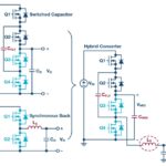
Proof-of-concept designs have been demonstrated for two GaN-based multilevel SC converters using a three-level buck converter topology. One is for 48Vdc server power supplies and the other is for 400V power factor correction (PFC) applications. Significant efficiency gains are possible for these power converters compared with a two-level topology. Smaller passive components (primarily the inductors, which can occupy up to 80% of the total volume in a two-level design) also provide an increase in power density for the server power supply. And the power supply benefits from improved thermal performance compared with a two-level design.
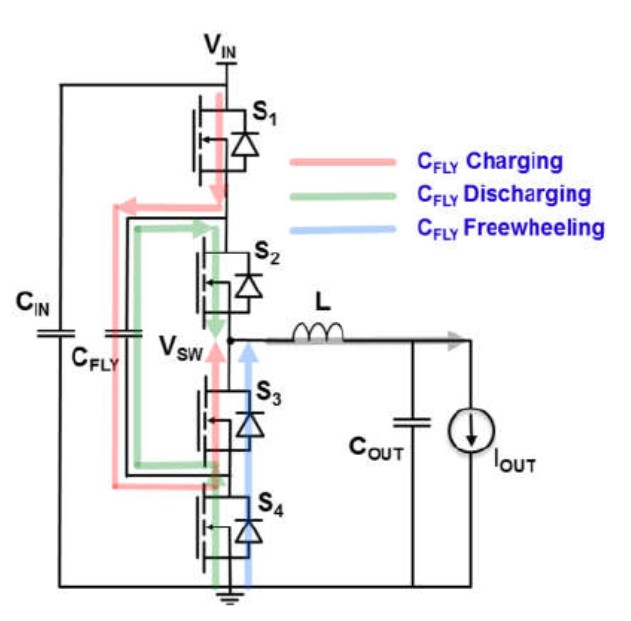
These three-level GaN-based SC converters demonstrate two novel multilevel gate drive schemes: a cascaded synchronous bootstrap gate drive that is suitable for integration in to a drive IC and a Zener diode-based bootstrap design for low-cost mass production. Flying capacitor (SC) balancing is implemented in both the 48V and 400V designs. In addition, the 48V design delivers good transient response to load changes. A Zener-diode startup scheme is used in the 400V design. GaN-based multilevel converters are expected to be efficient and reliable alternatives for a variety of applications including stacked energy buffer circuits and synchronous rectification.
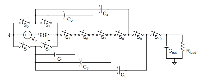
Another team of researchers has demonstrated an interleaved 1-to-6 step-up resonant SC converter using GaN power devices. The design uses a Dickson SC converter with two modules operating 180° out of phase. A split-phase control scheme with resonant operation is used to implement zero current switching. The converter provides 20V to 120V conversion with 95.7% peak efficiency and inherent current sharing within 10% over all conditions between the two phases. The converter delivers a power density of 314 W/in3.
A GaN-based transformer-less microinverter with extended duty ratio (EDR) boost as the dc/dc stage has been developed. As an SC-based interleaved boost converter, the EDR provides high gain and reduces the voltage and current stresses on most of the power switches. The interleaved inductor currents reduce the equivalent ripple on the converter input current and the power loss in the inductor. As a result of the dynamically variable DC line (EDR) the voltage swing seen by the decoupling capacitor is reduced, allowing the use of all film capacitors. This 100kHz, 300W microinverter produces an output of 120Vac, 60Hz from inputs ranging from 20 to 40 Vdc.
GaN-based SC dc/dc resonant boost converter
A GaN-based 400W dc/dc resonant SC voltage doubler (SCVD) has been developed that uses zero-current switching. Turning off the switch shortly before the zero-crossing of the oscillating current and turning on the other switch during reverse conduction results in high-efficiency operation. The key to achieving this performance is the use of sufficiently fast switches. In this design, GaN switches are used because of their fast switching speeds. In addition, the linear relationship between output capacitance and drain-source voltage in GaN devices can be used to improve the shape of the currents in oscillating circuits. The lower RDS(on) increase versus temperature for GaN devices enables operation at a higher temperature and higher efficiency compared with silicon devices. The smaller area of GaN devices compared with silicon switches contributes to higher power density and the low gate charge of the GaN switches improves converter operation.
The maximum efficiency that was measured for this 200V to 400V converter exceeded 99.2%. Using a synchronous control scheme enables bi-directional power conversion, making this design suitable for battery systems, particularly in electric vehicles or grid-connected energy storage. This design uses a planar choke and small GaN power switches to achieve both high efficiency and high power density.

SC converters for EV and HEV battery cell balancing
In addition to bi-directional conversion for EV battery and grid-connected energy storage battery packs, SC-based bi-directional power conversion can be used for cell balancing within the packs. Sometimes called equalization, cell balancing is critical to ensure reliable long-term operation of high-voltage battery packs. The use of SC bi-directional dc/dc converters can reduce cell balancing times and the number of switches needed to implement cell balancing.
In some EV designs, ultracapacitors (UCs) are used to supplement the main Li-ion battery pack. The main battery pack supplies the large energy needed for motive power while the UC pack can contain up to 600 UCs and is used to supplement motive power during acceleration and to rapidly absorb power during regenerative braking. The combination of batteries and UCs improves battery lifetimes and reduces the size and weight of the overall energy storage system. A bi-directional SC converter has been developed for battery and UC equalization and balancing.

The SC converter transfers power from a higher voltage cell to a lower voltage one. There are three modes of operation: charging, discharging and idle. During charging and discharging, dynamic control is used to maximize pack operation. During idle, cell balancing is performed as needed. Using an SC based converter for battery and/or UC cell voltage equalization has three advantages: reduced losses in the power switches, lower electromagnetic emissions and reduced size, cost and weight of the overall energy storage and management system.
Grid-scale SC converters
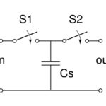
New SC topologies are being proposed for high power applications such as high voltage interconnects for offshore windfarms and multi-terminal high-voltage DC (HVDC) transmission systems. One example of high-power SC developments is the SC multilevel inverter (SCMLI). The SCMLI has the benefit of a lower dc supply requirement and can operate in both symmetric and asymmetric modes, but it is complex and is made practical by the availability of low-cost, high-performance microcontrollers. The SCMLI has a smaller number of switching devices for a given output voltage compared with other topologies, but its operation generates thirteen and thirty-one level output voltages for symmetric and asymmetric selection of dc voltage sources, respectively.
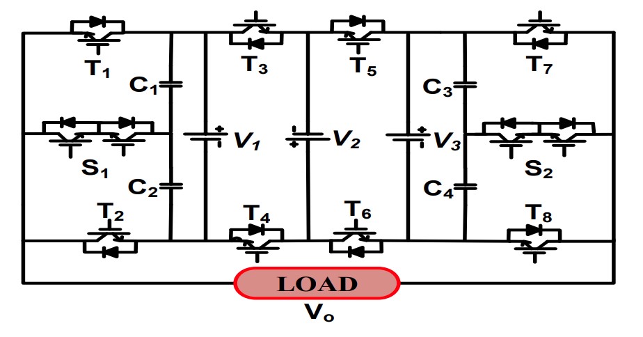
Referring to the image above, the SCMLI has eight unidirectional switches (T1 to T8), two bidirectional switches (S1 and S2), three DC voltage sources (V1 to V3) and four switched capacitors (C1 to C4). The switch pairs, T3 and T4 and T5 and T6 are complementary, to avoid short circuiting the dc voltage supply. By varying the levels of V1, V2 and V3, the same topology can be configured for asymmetrical and symmetrical operation. The SCMLI uses nearest level control (NLC). NCL approximates the reference voltage with the nearest voltage level, enabling more voltage levels and resulting in a fundamental switching frequency with the lowest switching losses. When used in high output voltage applications, NLC minimizes the switching losses and lower-order harmonics. NLC control can operate at 50/60 Hz and is extendable to N-levels.
That concludes this FAQ series on switched capacitors. SCs are highly versatile circuit elements with applications ranging from analog signal chain uses to power conversion and from very low power portable devices and wearables to utility-scale applications. You might also be interested in reading part 1 of this series on “Switched capacitor filters, amplifiers and integrators” and part 2 on “Switched capacitor power conversion for electronic systems.”
References:
A Gallium Nitride Switched-Capacitor Power Inverter for Photovoltaic Applications, Ohio State University
A Novel Switched-Capacitor Multilevel Inverter Topology for Energy Storage and Smart Grid Applications, MDPI
Charge Pump, Wikipedia
Design of GaN Based Multilevel Switched Capacitor Converters – Benefits and Challenges, Researchgate
Fixed Ratio High Power Inductorless (Charge Pump) DC/DC Controller, Analog Devices
GaN-Based DC-DC Resonant Boost Converter with Very High Efficiency and Voltage Gain Control, MDPI
Interleaved 1-to-6 Step-Up Resonant Switched-Capacitor Converter Utilizing Split-Phase Control, U.S. Department of Energy Office of Scientific and Technical Information
Switched capacitor DC-DC converters for HVDC applications, Researchgate
Leave a Reply