
Schottky diodes are useful in some power-converter topologies, especially for shunting the body diode in a half-bridge’s low-side MOSFET. In this position, the Schottky diode prevents the body diode from turning on, particularly when driving inductive loads common in power converters, because it’s forward voltage drop is smaller than that of the body diode’s PN junction. And that’s the single attribute for which Schottky diodes are best known: Low VF.
But, beyond exhibiting diode-like behavior, Schottkys are quite different from their PN-diode cousins. For starters, from the simplest discreet device to the most complex integrated circuit, nearly all metal-semiconductor interfaces are engineered as ohmic contacts that exhibit linear, bidirectional V-I characteristics. This critical trait ensures that device electronic behaviors are determined by semiconductor geometries and doping profiles and by other processed features such as the shapes, extents, and deposition thicknesses of films that form integrated resistors and capacitors. A goal that runs throughout semiconductor process design is to ensure that, at most, parasitics associated with metal interconnects only minimally affect circuit behaviors. Not so with the Schottky.
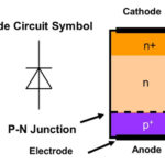
Fabricators form a Schottky diode with a non-ohmic metal-semiconductor interface at the anode end. A typical arrangement is a metal contact to a lightly doped N-type semiconductor. The doping profile depends upon the specific device design but, in all cases, varies across the semiconductor’s length to ensure formation of an ohmic contact at the cathode end of the diode. Typical forward voltages are in the range of 300 to 400 mV compared to silicon PN diodes which exhibit forward drops of 600 to 800 mV or more.
The Schottky’s final forward voltage is a function of material choice — both the metal and the semiconductor — and the semiconductor doping level at the metal interface. Although conceptually attractive and chemically possible, engineering Schottkys for lower forward voltages also boosts the reverse leakage currents, which tend to be higher than those for PN diodes anyway. For a given application, the relative efficiency improvement provided by a low VF should be compared to the losses incurred by the reverse leakage and, because both accrue as integrals in time, the circuit’s duty cycle and its arithmetic compliment are factors in the respective calculations.
 Diodes model statically as an ideal junction in series with a series potential drop, a series resistance, and a leakage term. As with virtually all semiconductor parameters, the forward voltage drop, series resistance, and leakage are nonlinear and functions of temperature. So models of them as traditional fixed linear quantities are first-order approximations. The forward voltage exhibits a negative temperature coefficient typically in the neighborhood of -1 to -2 mV/°C. The diode internal resistance is also a function of temperature. But the overall thermal characteristic is dominated by the forward voltage tempco.
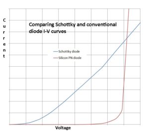 The series resistance, also a function of semiconductor doping, is larger than that for PN diodes. This larger series resistance results in I-V curves with slopes shallower than those for PN diodes. Quantitatively, the trajectories depend on the specific device designs so your mileage will vary. The point here is that, as a rectifier, the Schottky’s efficiency advantage of low VF can be limited to modest currents.
As a clamping device, however, the Schottky is highly effective because its impedance in most applications is not as strong a factor in the circuit’s overall performance as its reverse recovery qualities. Unlike the PN diode, there is no carrier recombination in a Schottky during the transition from conducting to blocking. The junction capacitance is smaller as well. The result is a reverse recovery dynamic that is as much as three orders of magnitude faster than in silicon PN diodes for small devices and two orders of magnitude faster for large diodes intended for high-power applications.


Clamping inductive loads and a fast recovery as well as a Vf at higher currents. I’m glad someone sent this information.