
A review of MOSFET advances helps predict where the technology is likely to head.
Ashita Mirchandani, Bastian Lang • Infineon Technologies
The past 50 years have seen unprecedented changes enabled by technology. The trend will continue with emerging technologies such as e-mobility, the Internet of Things (IoT), artificial intelligence, connectivity and 5G. At the heart of these emerging technologies is cutting-edge innovation in MOSFET technologies that provide power.
These new application areas are increasingly power hungry, challenging MOSFET designers to adapt new power architectures and higher bus voltages. There’s also a need to deliver power more efficiently in ever-smaller form factors. For example, today’s smart phones provide many more features than cell phones from years past but in a comparably sized package.
When faced with these new challenges, designers must keep the customer’s end application in mind. Evaluation should incorporate test conditions identical to those in the environment where the device is to be used. In these cutting-edge applications, use of the right power switches often determines system performance.
Innovations in MOSFET technology that handle emerging applications are not a new phenomenon. Consider the first hexagonal topology MOSFETs in 1979, known also as HEXFET. This technology enabled the rapid commercialization of switch-mode power supplies. Similarly, a new MOSFET technology in 1995 was based on an advanced four-mask process using innovative self-alignment features to improve manufacturing precision and yields. It lowered MOSFET manufacturing cycle time and allowed junction depths up to 40% shallower than before, reducing the transistor junction resistance while boosting ruggedness. Shortly afterwards, the first FETKY was introduced. (Basically, a co packaged HEXFET and Schottky diode). The single silicon FETKY chip reduced the form factor and losses in dc-dc applications.
In 1999, a stripe planar technology was perfected that featured an extremely low on-resistance, excellent high-frequency operation, ruggedness and low manufacturing cycle time. The same year, a family of Trench power MOSFETs enabled industry’s highest cell density and lowest RDSon. This technology focused on delivering high energy efficiency for handsets, laptops and other portable electronic devices.
The year 2000 brought the first family of OptiMOS MOSFET technology featuring ultra-low switching losses for high efficiency. The OptiMOS family is now in its sixth generation, with each family further reducing RDSon and improving switching performance. Applications such as synchronous rectification in switched-mode power supplies (SMPS) for servers, desktop PCs, wireless chargers, quick chargers and OR-ing circuits now use the technology.
In 2021 came the StrongIRFET family. These MOSFETs are optimized for low RDSon and high current, making them candidates for low-frequency applications requiring ruggedness such as cordless power tools, light electric vehicles and e-bikes.
Packaging is also an important aspect of power products. In 1993, the SOT-223 was introduced as the first surface-mount power MOSFET. In 2002 came the DirectFET power package, a proprietary surface-mount format with a new interconnection methodology bringing radical gains in both conduction and thermal efficiencies. The widely used TO-Leadless package came in 2013. It handles high current in a reduced foot-print compared to a traditional D2PAK. Most recently, Infineon has devised a family of OptiMOS power MOSFET devices in a PQFN 3.3×3.3 Source-Down package (the IQE006NE2LM5) with a flipped die for better thermal performance and lower RDSon.
Future developments
Innovations in power delivery and packaging continue to enable new applications. Consider artificial intelligence. Power management–more specifically, the energy density of the power converters fueling processors and ASICs–is a big challenge for designers. The introduction of 48-V bus voltage allows additional power conversion close to the payload to avoid transmission losses.
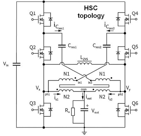
With Infineon’s Hybrid Switched Capacitor (HSC) resonant dc-dc converter, innovative components brings new capabilities to the whole system. The HSC is formed by six MOSFETs divided into two legs, connected through two flying capacitors and a magnetic device called a multi-tapped autotransformer (MTA). The MTA is formed from four windings connected in series sharing the same magnetic core.
High-frequency operation is enabled by ZVS (zero-voltage switch) operation with the magnetizing inductance of the MTA. The HSC provides an unregulated voltage rail which depends on the turns ratio between the MTA primary windings N1 and N2. The topology is driven by two symmetrical PWMs dubbed H (i.e., Q1, Q3 and Q5 are ON with Q2, Q4 and Q6 OFF in the nearby topology diagram) and L (i.e., Q1, Q3 and Q5 are OFF with Q2, Q4 and Q6 ON). An introduced dead-time between the states enables load-independent ZVS operation. The HSC can run above- and below-resonant frequency without influencing the ZVS operation. Therefore, the overall system performance can be kept at a high level regardless of component tolerances.
One of the key enablers for high efficiency and high power density of the HSC is the use of low-voltage rated MOSFETs with better figure-of-merits (FOMs). For example, in an 8:1 configuration running from a 48-V rail, 25-V-rated MOSFETs for Q3 and Q6 can be used.
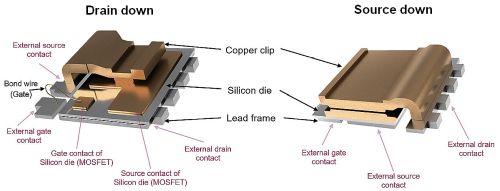
Combined with new Source-Down products, the HSC can provide the power density needed in modern data centers. Main benefits of the package include 30% lower RDSon, lower package-related parasitics and lower Rthjc. As the thermal pad is located on the source pin, the package enables optimized layouts where the large GND area can be used as a heatsink.
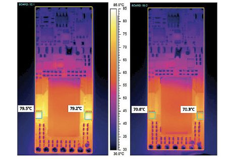
The performance benefits can be visualized from the comparison of two 8:1 HSC converter boards. One is based on a standard Drain-Down device (BSZ011NE2LS5I) and the other on the new Source-Down device. A hotspot can be observed in the traditional package but not in the new Source-Down package. The surface temperature of the MOSFET is significantly lower, showing a 9°C difference compared to the Drain-Down device. The higher efficiency of the system incorporating the Source-Down device leads to a significant increase in power density as well.
The development of MOSFETs and packaging will

continue to evolve. MOSFET technology continues to power emerging technologies through new innovations. While there is tremendous potential for wide bandgap (WBG) devices such as SiC and GaN, silicon is still the mainstream choice for many applications. Silicon and WBG materials will both play a role in power switching. New innovative MOSFETs power the latest applications and continue to be “cool.”


Leave a Reply