
Depletion-mode MOSFETs have qualities that let them work well in several kinds of power-handling circuits.
Aalok Bhatt, José Padilla, Raymon Zhou • Littelfuse, Inc.
Most MOSFETs are enhancement-mode (EM) devices: When their gate-source voltage is zero, they don’t conduct. When the need is for a switch that is normally on when there is no power applied, depletion-mode (DM) MOSFETs fit the bill: When their Vgs = 0 V, they conduct. Unlike EM devices, DM devices don’t find use in high-speed switching. Nevertheless, there are numerous applications where DM devices come in handy. It is worth examining the properties of these less well-known MOSFETs.
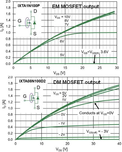 As mentioned, EM MOSFETs have no conduction at Vgs = 0 V. Conduction starts at gate-to-source threshold voltage VGS(th). For the EM device, the drain current ID rises when Vgs >VGS(th). The EM device ceases to conduct at Vgs <VGS(th). In contrast, current in the DM device rises when Vgs >0. A negative gate voltage Vgs reduces the current ID, and the device stops conducting at gate-to-source cut-off voltage VGS(off).
The fact that an EM device doesn’t conduct at Vgs = 0 V means it cannot directly replace a DM device. An additional point to note is that some DM applications need no gate-drive circuit because the gate gets biasing from the circuit in which it is implemented. Thus the use of DM devices can reduce complexity and costs while improving reliability thanks to the ability of DM MOSFETs to operate in linear mode.
Usually, EM devices are incapable of linear mode operation, except for linear MOSFETs. (As a quick review, MOSFETs operating in the linear region have an ID governed only by VGS and which remains constant for any given VDS. In other words, the MOSFET behaves like a constant-current sink. In this operating mode, MOSFETs typically dissipate higher power than when they are switching because of simultaneous high voltage and current. Ordinary EM MOSFETs designed for switching may not last long if they operate in the linear region.
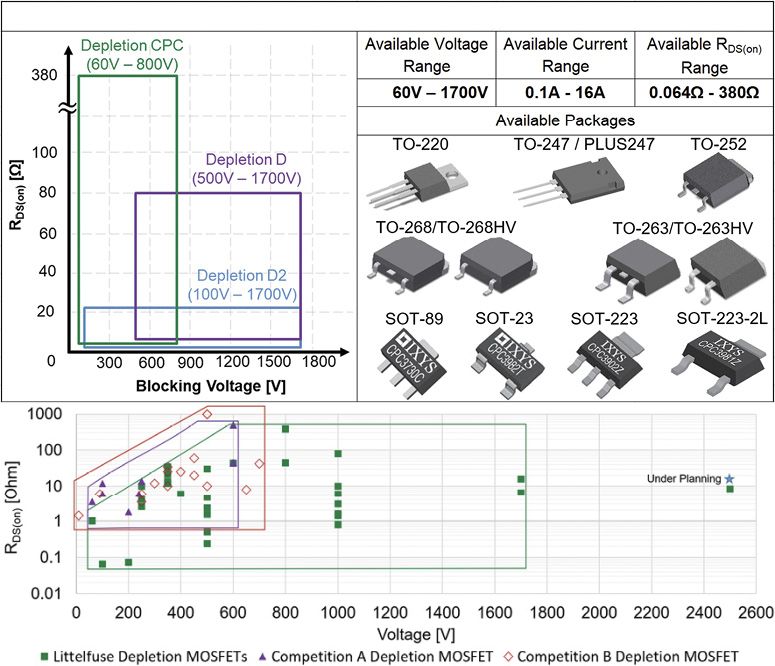
High-voltage DM MOSFETs with 2,500-V ratings are currently under development. Typical applications for these devices are in high voltage (HV) test equipment, power supply, ramp generator, insulation resistance test equipment, and auxiliary power supplies for HV power transmission systems.
Applications of DM MOSFETs
It may be useful to examine a few applications that are particularly suited to DM MOSFETs. First consider the start-up circuit of a switched mode power supply (SMPS).
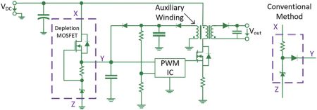
Here the conventional start-up circuit uses a power resistor and a Zener diode sitting in parallel with the load. In this approach, the power resistor continuously consumes power after the start-up phase. The result is excessive heat on the printed circuit board (PCB), poor efficiency, and an SMPS with limited input voltage operating range.
Alternatively, a DM MOSFET can provide the initial current required by the PWM IC to kick-start the operation. After the start-up phase, the auxiliary winding will generate the necessary power for the PWM IC. During normal operation, the depletion MOSFET draws minimal power because of its low quiescent current.
The main advantage of this approach is theoretically zero power dissipation after the start-up sequence thus improving overall efficiency. Moreover, the resulting circuit takes up a smaller area on the PCB. It also handles a wide range of dc input voltages, essential for many applications such as solar inverters.
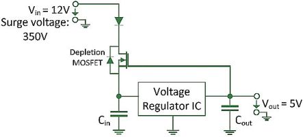
Another DM application to consider is surge protection for linear voltage regulators. Linear voltage regulators power small analog circuits, CMOS ICs, and other loads requiring low current where the input voltage Vin comes directly from a bus voltage. This power arrangement might have significant voltage variations, including high-voltage spikes due to the application environment.
Here the DM MOSFET is typically connected in a source follower configuration: The voltage on the source follows the voltage on the gate. The DM MOSFET conduction depends solely on its gate voltage and is independent of its drain voltage. This configuration will mitigate any voltage transient up to the withstand capability of the device voltage rating VDS.
The advantage of a DM MOSFET here is it makes possible a wide dc operation voltage range Vin and minimal power dissipation thanks to the low MOSFET quiescent current. Such protection comes in handy for mitigating transients caused by lightning strikes in telecommunication circuits. A similar use is in automotive and aviation electronics to mitigate transients caused by inductive loads.
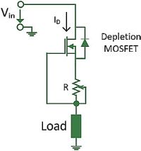
Additionally, DM MOSFETs can be the basis of constant current sources. This circuit supplies a constant current to the load depending on the value of a resistor in series with the load and the gate cut-off voltage VGS(off). The drain current is thus independent of the input voltage. Current source circuits can be found in LED array drivers, trickle charger circuits maintaining battery charge, or to charge capacitors at a constant rate.
Another DM constant-current application to consider is the high-voltage ramp generator which basically constructs a ramp voltage via an RC circuit. Automatic test equipment, as an example, require high-voltage ramps with a linear relationship between output voltage and time. The constant current source charges a capacitor via a

resistor and generates a voltage ramp across the capacitor. A linear MOSFET connected in parallel with the capacitor can be turned on with a control signal to discharge the capacitor and thus reset the ramp voltage.
The next example is in high-voltage protection circuits. A DM MOSFET can protect measurement instruments from the accidental connection of measurement probes to high voltages. The typical configuration has two MOSFETs configured back-to-back with a resistor in between them. Each MOSFET gate is connected to the source of the other MOSFET. This approach protects the instrument by limiting the current. Bench-top or hand-held instruments a potential applications.
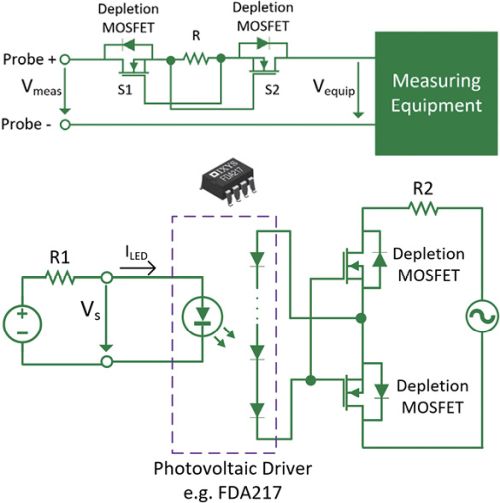
Depletion MOSFETs are also excellent for implementing solid-state relay (SSR) load switching in place of electromechanical relays (EMR). SSRs provide immunity to magnetic fields, high reliability due to the absence of mechanical contacts, smooth operation thanks to the elimination of contact chattering, and take up less space than EMRs on PCBs. SSR applications include medical equipment, industrial automation, consumer electronics, and measurement and test equipment.
Although DM MOSFETs are almost forgotten, they can be useful whenever there is a demand for current at zero gate voltage. Littelfuse has the widest range of these, from 60 to 1,700 V and is the only manufacturer offering high-current DM MOSFETs.
References
Straight facts about linear MOSFETs and their applications; Bodo’s Power Systems, October 2021.
White paper, MOSFETSs withstand stress of linear mode operation, 2021, littelfuse, Inc.
White paper, Depletion-mode power MOSFETs and applications, Abdus Sattar, Ixys corp.
Littelfuse DM MOSFETs, gate drivers


Leave a Reply