
Regulatory creepage and clearance requirements are increasingly affecting mainstream designs; understanding and meeting them is a complicated, multifaceted process.
The final part of this article looks at an IC pair specifically designed for an enhanced creepage and clearance value, tools for helping with design, and also provides some “pre-electronics” perspective on the subject.
Q: Are there ICs specifically designed with creepage and clearance in mind?
A: Yes, there are quite a few available from vendors with expertise in analog components and reinforced-isolation fabrication. Most reinforced isolated amplifiers come in a SOIC package with less than 9 mm of clearance and creepage specification. However, systems with working voltages greater than 1000 VRMS, impulse voltage requirements greater than 8000 V, for altitudes greater than 2000 meters, or a pollution degree 2 or higher may require clearance and creepage distances greater than 9 mm depending on the overvoltage category of the designed system.
Q: Can you provide an example?
A: Texas Instruments, among other vendors, offers two similar ICs specifically designed for meeting these higher creepage and clearance requirements at higher voltages. These are the AMC1411 (for voltage sensing) and AMC1400 (for current sensing) high-performance isolated amplifiers with reinforced insulation (Figure 1).

These products come in a stretched-SOIC (double width or DWL) package with clearance greater than 14.7 mm and creepage of over 15.7 mm. They are specifically designed for use in high-voltage, high-altitude, and high-pollution degree environments.
Q: Figuring all this out on a PC board layout seems very complicated and error-prone; are there tools that can help?
A: Yes, there are. As one example, the Constraint Manager in Cadence’s Allegro PCB Editor can be set up with a specific package to package clearances to maintain the proper creepage spacing of high-voltage parts. In addition, you can also create net classes for power and ground nets and assign them the necessary spacing clearances as well.
Q: What happens next with this tool?
A: Once you have the spacing requirements that the board will need for proper creepage and clearance, these values can be set up in the PCB-layout system’s design rules. These include ‘Rules and constraints” for metal-to-metal clearances, which can be between traces, pads, copper pours, or any combination of the three. You can even set up unique keep-out clearances around specific footprints to account for heat sinks and other unusual configurations. All of these rules allow you to maintain the necessary spacing between high-voltage components.
Q: Does this sort of tool solve the entire problem?
A: No, it does not. Care is still required, as you must ensure that any edits or changes to the component placement don’t end up violating spacing that you have already carefully set up between the parts. A simple act such as rotating a component 90 ° can cause an unusually shaped part to violate a voltage clearance.
Q: These tools are helpful, but it all still seems to be very complicated. Is there another solution?
A: Yes, it is often easier or smarter (or both) to hire a consultant who is an expert in the many rules, requirements, subtleties, and exceptions related to creepage and clearance. An experienced consultant can not only find “problems” with your design or layout but also suggest alternatives to overcome potential problems and explain the tradeoffs of each one. In today’s advanced board layouts, even a small change to solve one problem, such as creepage and clearance, may have an unintended or unforeseen “ripple effect” on another problem, such as EMI/RFI performance, or vice versa.
Understanding the options to address one problem may give you the degrees of freedom needed to not aggravate the latter one in the course of doing so. A specialized consultant versed in creepage and clearance (as well as those for EMI/RFI design and certification) can save you a lot of time and aggravation, especially as the regulatory mandates are difficult, complex, and confusing.
Q: This entire creepage and clearance issue seems like a relatively new thing, but is it?
A: Yes and no. It has only become a problem for PC boards in the last few decades as boards have become denser while voltages in some cases have increased. But the overall problem was known before the “electronics” age by engineers working on power lines, and we still see the results of their work every day.
Q: How so?
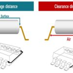
A: Look at almost any power line and its poles, supports, and towers to which it is attached, and you’ll see large insulators separating them from their support and each other (Figure 3). This applies to modest 120/240 VAC lines as well as those into tens of hundreds of kilovolts. The insulator size scales up with the volage, of course.

The insulators are shaped with “scoops” or corrugations to maximize creepage and clearance while providing the basic mechanical strength needed. A rough estimate of the creepage distance required in clean air may be 15 millimeters per kilovolt (line voltage). The required creepage distance increases in the polluted air, depending on the level of pollution.
Q: Of what are these high-voltage insulators made?
A: These insulators have traditionally been made from sophisticated ceramics and glazing, and many still are made using those materials. However, polymer or composite insulators are increasingly used in high-voltage transmission systems. The polymer insulators have a fiber rod surrounded by an outer sheath of one of various polymers. Due to the hydrophobic nature of the polymer insulator surface, dry areas are formed between wet areas, resulting in discontinuities in the wet-creepage path. This phenomenon helps improve the performance of the polymer insulator in polluted and coastal areas. But it’s a tradeoff, as polymer insulators age faster than ceramic insulators, especially in harsh or salty-air environments.
Conclusion
Creepage and clearance are two closely related, critical design requirements that become issues as voltages exceed around 30 VAC or 60 VDC. Meeting them requires a careful understanding of their multiple complicated regulatory mandates as well as attention to design detail with respect to layout, component selection, component and board trace placement and orientation, and more. While CAD tools are available to assist in this effort, outside help from an experienced specialist may be needed to ensure the final design meets the requirements.
Related EE World Content
Key considerations when integrating high voltage dc-dc converters into critical applications
Why I was scared by a technical article
With so many mandates, can successful designs still be achieved?
Why and how are medical connectors and standards different?
Power supply regulations, requirements, and standards
Navigating new safety standards for power supplies
Coming: New safety ratings for power adapters
The basics of AC-line isolation for safety, Part 1: The challenge
The basics of AC-line isolation for safety, Part 2: The solution
External References
Samtec, “Clearance and Creepage” (very useful and has additional linked references)
Cadence Design Systems, Inc., “Designing to High Voltage Creepage and Clearance Standards in Circuit Board Layouts”
Coil Technology Corp., “What is clearance and creepage distance of insulation?”
Weidmüller Interface GmbH & Co. KG, “Creepage and clearance distances”
Sierra Circuits, Inc., “The Importance of PCB Line Spacing for Creepage and Clearance”
Texas Instruments, “How to Meet the Higher Isolation Creepage & Clearance Needs in Automotive Applications”
Texas Instruments, “TI’s First Isolated Amplifiers With Ultra-Wide Creepage and Clearance”
Excelsys Technologies, “Design Considerations for Power Supplies in High-Altitude Applications”
Advanced Energy, “How to Select Power Supplies for High-Altitude Applications”
NS Transmission Pvt. Ltd., “High Voltage Insulator”
ADAPT Australia, “Extension Insulators and Extension Link Insulators 15 kV to 69 kV”
Leave a Reply