Silicon carbide (SIC) MOSFETs and silicon (Si) IGBTs can both boost sustainability in green energy systems. Of course, they don’t compete across the board, there are uses where one or the other is clearly preferred. When comparing the two technologies, it often comes down to the prioritization of performance characteristics like light weight versus low cost. And both technologies continue to get better.
Si IGBTs are a mature technology and are advancing at a slower pace, while SiC MOSFETs are improving more rapidly. That can increase the complexity associated with making a choice between the two. This FAQ briefly looks at the changing tradeoffs between Si IGBTs and SiC MOSFETs, reviews some benefits of using Si IGBTs, some challenges associated with using SiC MOSFETs in green energy applications, and closes by looking at advanced gate drives for SiC MOSFETs and advanced gate structures for Si IGBTs.
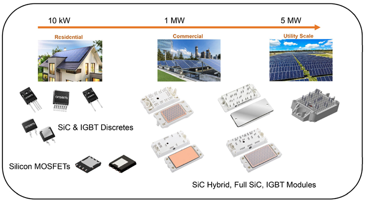
The choice is not simply Si IGBT versus SiC MOSFET; there is a continuum of options. In the case of solar energy systems, for example, low-power residential systems can choose between discrete Si and SiC MOSFETs and Si IGBTs. As the power level rises to commercial systems up to about 1 MW, the choices change to various types of modules including Si IGBT modules, hybrid modules with Si IGBTs, SiC diodes, and full SiC modules. At grid-scale power levels, high-voltage Si IGBT modules dominate (Figure 1).
The goalposts are moving
As in most areas of technology, Si IGBTs are being continually refined to better suit specific application needs. For example, in the case of commercial and grid-scale PV systems, bus voltages of 1.5 kV are being used in some designs to improve system efficiency. The highest voltage an IGBT must block shouldn’t exceed 80% of the VCES rating. Common IGBT module voltage ratings like 1.7 kV are limited to use with voltages up to about 1.3 kV and are not suited for use in most 1.5 kV PV systems, and 3.3 kV modules suffer from over-specification.
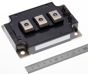
Using 1.7 kV or lower rated IGBT modules in 1.5 kV bus systems requires a more complex design like a three-level neutral point clamped (NPC) topology that guarantees voltage sharing across modules. To address the emergence of higher voltage buses, IGBT modules have been developed rated for 2.0 kV. With derating, they can handle 1.6 kV and are suited for use with the new 1.5 kV buses. The 2.0 kV modules enable the use of simpler topologies resulting in smaller and less expensive 1.5 kV rated PV inverters (Figure 2).
At the same time as IGBTs are being refined, SiC MOSFETs are evolving. In one case, a 2 kVA single-phase inverter was implemented using IGBTs and 1,200V discrete SiC MOSFETs. The total losses (conduction + turn on + turn off) were about 41% lower for the SiC MOSFET design compared with the IGBT implementation, falling from 14.4 W using the IGBT to 5.9 W with the SiC MOSFET. Of course, the performance of SIC MOSFETs is improving at a more rapid rate compared with Si IGBTs and the performance gap is widening accordingly.

When to use IGBTs?
IGBTs are suited for applications that benefit from medium-speed switching, need high voltages, low cost, and are not particularly sensitive to overall system size. It’s not just IGBTs versus SiC MOSFETs; in several types of inverter applications, like consumer white goods, IGBTs can be competitive with Si MOSFETs. Those applications are more sensitive to cost than maximum thermal performance. In other applications, thermal management can become a limitation for Si IGBTs. It’s not a simple ‘either or’ choice between power devices.
Si IGBTs and SiC MOSFETs are voltage-driven devices; an IGBT structure consists of a MOSFET driving a bipolar transistor. The bipolar nature of IGBTs enables them to carry high currents with low saturation voltages and low losses. SiC MOSFETs also have low conduction losses but have limited voltage ratings compared with Si IGBTs. For high-voltage and high-power applications, IGBTs are the preferred solution. On the other hand, SiC MOSFETs are more thermally rugged making them more suited for high-temperature environments.
In medium voltage applications, where the choice is between Si IGBTs and SiC MOSFETs, the higher losses associated with IGBTs can become a significant consideration. Thermal management raises the cost of using IGBTs, and their slower switching speeds can increase the cost of passive components like capacitors and inductors. But even then, the overall system cost is not a simple equation.
Using SiC MOSFETs in green energy systems
It’s not simply a matter of replacing Si IGBTs with SiC MOSFETs. The use of SiC MOSFETs requires a different design approach, resulting in a learning curve for designers unfamiliar with the technology, increasing the design risk and potentially delaying time to market. Those are some of the factors delaying the adoption of SIC MOSFETs, even in applications that may be able to benefit from the performance improvements they offer. For example, printed circuit board (PCB) design is an important factor in power converters and SiC MOSFETs have different PCB needs compared to Si IGBTs. Some examples include:
- Faster switching speeds produce faster di/dt and dv/dt slew rates. That means designers need to consider factors like false turn-on, parasitic resonances, cross talk, and increased electromagnetic interference (emi).
- PCBs for SiC MOSFET power converters can be smaller, but they still require the same creepage and clearance distances required for all power converters. It’s not just the devices; the smaller heatsinks they use can also impact creepage and clearance performance.
- Efficient driving for SiC MOSFETs is also important and different compared with IGBTs. Faster switching is again the culprit. A tight gate drive PCB layout is needed to minimize undesired characteristics like oscillations, overshoots, emi, and other factors. Low inductance drive loops are important, and parasitic capacitances need to be minimized.
SiC gate drive optimization
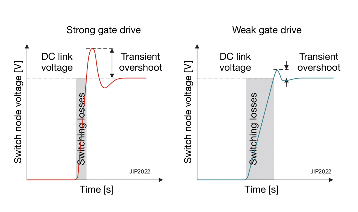
Gate drive optimization is important to maximize the performance of Si IGBT and SiC MOSFETs. In the case of SiC MOSFETs, it’s necessary to minimize switching and conduction losses during turn-on and turn-off. With conventional gate drivers, there can be a tradeoff between faster switching speed and increased transient overshoot. Recently, an adaptive drive scheme has been advanced for SiC MOSFETs that addresses that tradeoff.
The new approach varies the gate drive current and enables overshoot management (Figure 3). It has been optimized for use in EV battery packs. For battery packs charged from 80% to 100%, a low gate drive strength can be used to optimize overshoot while maintaining efficient SiC MOSFET operation. When supporting packs between 80% and 20% of full charge battery chargers can benefit from a high-strength gate drive to reduce switching losses. By optimizing the gate drive current between 5 and 20 A, a 2% overall efficiency increase can be realized for EV battery chargers.
Three IGBT gates can be better than one
IGBTs have been highly refined over many years making it increasingly challenging to realize significant improvements in performance. For example, it’s difficult to reduce overall power losses since in a conventional IGBT design, reducing conduction losses generally leads to increased switching losses.
A lot of the challenge is from the tail current attributable to minority carriers when an IGBT turns off. As the device turns off, the depletion region expands, increasing the collector-emitter voltage and the minority carriers become part of the internal recombination current, that’s the tail current that appears during the later stages of turn off and is a significant contributor to switching losses. To reduce switching losses, IGBTs are designed with an ‘optimal’ mix of minority carrier lifetime and the number of holes injected from the collector. Both these approaches increase on-state resistance. A third option has been recently proposed.
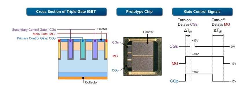
To improve IGBT switching performance and maintain low on-state resistance, it’s been proposed to replace the single gate with three gates, a main gate (MG), and primary and secondary control gates, CGp and CGs, respectively (Figure 3). When turning the triple gate IGBT (TG-IGBT) on, MG and CGp are turned on simultaneously, and CGs is delayed and is on for a brief period. It’s been demonstrated that turning the gates on in that order results in large electron and hole flows, turning the device on faster with lower turn-on losses. When turning the device off, CGs remains off, and CGp is turned off before MG. When MG turns off, the electrons and holes are quickly removed, reducing turn-off losses. Using the proposed three-level gate drive technique with a prototype 1.2 kV TG-IGBT resulted in 66% lower turn-on and 35% lower turn-off losses compared with a conventional device structure.
Summary
SiC MOSFETs continue to improve and are increasingly encroaching on applications dominated by Si IGBTs. At the same time, IGBT performance is improving, but at a slower pace. In addition, new gate drive approaches are being developed for both types of devices. The choice between Si IGBTs and SiC MOSFETs will remain a complex and important decision for the foreseeable future.
References
2.0kV IGBT Module for Industrial Use, Mitsubishi Electric
Designing with Silicon Carbide for High Efficiency Renewable Energy Systems, Wolfspeed
Getting the most out of IGBTs is about knowing When, Where and How to Use Them, onsemi
How to maximize SiC traction inverter efficiency with real-time variable gate drive strength, Texas Instruments
IGBT & SiC Gate Driver Fundamentals, Texas Instruments
Three-level Gate Drive Technique for Enhancing Switching Loss Reduction in Triple-Gate IGBTs, 2022 IEEE 34th International Symposium on Power Semiconductor Devices and ICs (ISPSD)
What are the merits of using SiC MOSFETs?, Toshiba


Leave a Reply