
Stacked-load schemes have made power conversion more economical in server racks. New developments in this technology promise to provide additional gains in efficiency.
Laszlo Lipcsei, Alexandr Ikriannikov, Di Yao — Maxim Integrated, now part of Analog Devices
Load currents continue to rise in server applications while rail voltages tend to drop. Consequently, the conduction losses on the PCB are becoming increasingly harmful. For example, a processor running at 0.8 V and 1,000 A can require 24 phases of voltage regulator power stages to convert from a 12-V input down to the 0.8-V of the processor. The power conversion loss can easily reach or exceed 10%. The voltage regulators often need to sit a few inches away from the MCU such that the I2R loss can become significant as well. And high-current ASIC packages can reach the ball grid array electromigration limit that can either limit the amount of current that can be delivered into the chip package or jeopardize the package reliability.
 The concept of stacked power elements and processing of the power difference are considered possible solutions to this problem. Series-stacked architectures reduce the high step-down voltage conversion ratio in conventional architectures. Differential power processing converters regulate voltages and compensate for mismatches between MCU currents. In particular, the Energy Exchanger concept looks promising, where only the power difference is processed. In this architecture, the average current is observed in the system rail, not the minimum current of the elements connected in series. Losses are generally proportional to the processed power, so lowering the processed power usually reduces losses. And the Energy Exchanger architecture can use different converters, including different capacitor circuits.
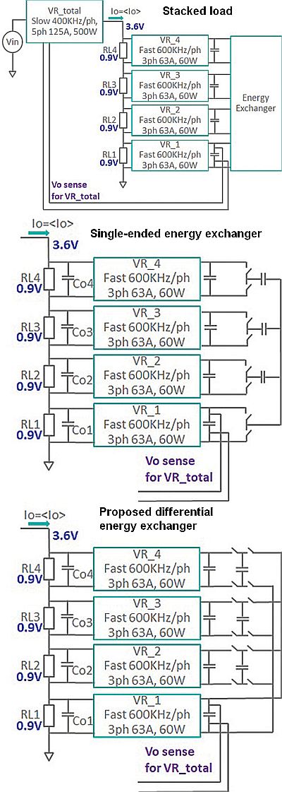
First a brief overview of the stacked power element and energy exchanger concepts. Power balancer circuits enable multiple load zones of an IC to be powered in series while maintaining balanced voltage at each load zone. The power balancer typically includes a dc transformer array consisting of a dc transformer connected in parallel with each load zone and for each load zone, a bus capacitor connected in parallel. Each dc transformer is electrically connected other dc transformers providing an electrical path for each bus capacitor to discharge current to other bus capacitors when a voltage across a bus capacitor exceeds a voltage across another bus capacitor.
Each dc transformer can include a switched capacitor circuit that includes a pair of switches such that when the first switch is on, the second switch is off and vice versa. A controller turns the switches on and off according to a specified duty cycle. The power balancer can include a voltage regulator for each load zone connected between the bus capacitor for the load zone and an input power connection to the load zone.
We can extend this concept to applications needing aggressive transient management. Voltage Regulators (VRs) are added to deal with the fast transient loads. A prototype board implements the single-ended energy exchanger with switched capacitor circuits. As you might expect, the single-ended Energy Exchanger showed significant noise pollution of the load rails when processing a significant power difference. Measured system efficiency was ~86% at full load of 250 W, with predicted ~2% improvement if the bias circuits are improved.
Visible in the block diagram of the Stacked Load prototype is the main Voltage Regulator VRR_total which delivers full power to the stacked loads as efficiently as possible. The four fast voltage regulators are responsible for the precise voltage regulation and transient response on each corresponding load rail. If loads are ideally matched, these fast VRs process zero power. They process a power difference only if there is a load mismatch. The fast VRs are thermally designed for much smaller current than VRR_total, as the maximum load difference is assumed to be smaller than the full load. However, it is important to design fast VRs so they can handle the full-scale transient of each load. Even if all loads are closely matched on average, it is hard to expect perfectly matched transient steps on all of them, and it takes longer for the slower VRR_total to adjust the output current.
The Energy Exchanger ensures power exchange among all the input rails for fast VR. If VRR_total is driving only linear loads connected in series, the output current is determined by the lowest load current. But when the Energy Exchanger is added, the VRR_total output current ideally becomes averaged current between all loads. In practice, that current is slightly higher as it compensates for the losses in the fast VRRs and Energy Exchanger.
Consider two different designs for the Energy Exchanger: the originally considered single-ended Energy Exchanger and a fully differential Energy Exchanger from.
The single-ended Energy Exchanger has a problem: Return currents from each flying capacitor must go through the Co bulk capacitors of the loads in series. These charge-discharge currents have a much faster ac content compared to the output currents of the buck converters (both VRR_total and fast VRRs). The simulated system performance with the single-ended Exchanger, when the load RL4 has a current step of 50 A, shows noise on all rails in general, which significantly rises when the Energy Exchanger starts moving charge to the input of VRR_4. The differential Energy Exchanger does not force any currents through the loads or the Co bypass of the load rails, fixing the noise problem.
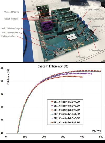
Two prototypes for the stacked load system were designed with the only difference being in the Energy Exchanger: one design contained the single-ended version, the second the differential Exchanger. Fast transient loads were used to evaluate the dynamic performance, implemented by pluggable modules.
Measured results
With load voltages at 0.8, 0.9, and 1.0 V, the two different Energy Exchanger options have nearly the same efficiency. In the nominal operating conditions, Vo = 4 x 0.9 V = 3.6 V reaches more than 95% at full load. Note that placing all loads in parallel corresponds to 500 A current into a single Vo = 0.9 V rail. Achieved >95% system efficiency noticeably outperforms published efficiency data for these conditions. Two main factors account for the high efficiency: 4x output current reduction as four loads are connected in series, and the main VRR_total delivers full power into 4x higher Vstack voltage (4 x Vo), as higher Vo generally improves VRR efficiency.
This is a prototype board with off-the-shelf parts and no optimized components; high efficiency is in part due to coupled inductors used in the main VRR_total, as well as fast VRR modules. Generally, coupled inductors keep switching frequencies low in a given reasonable size, keeping the switching loss down. This is especially important for the fast VRRs, because in the case of balanced loads, these VRRs do not process much power but still have switching losses that ideally should be minimized.
The big difference in the operation of the two different Energy Exchangers is in voltage ripple on all the first Vo1 rail and VR1 input supply rails. The Vo4 rail is loaded by I0 = 50 A, and all other rails are at zero current. So the Energy Exchanger is moving a lot of power from the other rails to supply the Vo4 rail. The single-ended Energy Exchanger drives large spikes through the parasitics of Co on the Vo1 rail while the differential Energy Exchanger just leaves the Vo rail intact, with only a small ripple at much slower time scale that relates to the buck converter currents (not the switched capacitor circuits).
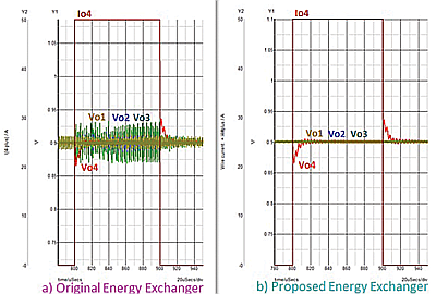
The most important impact is the reduction of the fast voltage spikes from >60 mV (>6.6% of Vo = 0.9 V) in case of the single-ended Energy Exchanger to <25 mV (<2.8% of Vo = 0.9 V) in the case of the differential version. In the latter case, the voltage ripple has no high-frequency spikes at all, only a ripple associated with the ripple current in the buck converters. The result matches the expected trend from the simulations. The fast spikes on the supply rail can potentially harm the digital circuitry, and it is important to mitigate the issue.
As Vo values are expected to drop further, the same amplitude of the noise has a larger impact on the operation of the fast loads. Noise in the differential Energy Exchanger can also be reduced by phase-shifting among switching events for the different flying capacitors. Notice this tactic is not possible for the single-ended circuit; all capacitors must be switched at the same times.
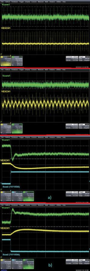
Fast transient performance is shown in the nearby figure for loading and unloading 100-A steps on rail Vo1. The other rails are unloaded. So, while initially the fast VRR1 delivers all 100 A, the averaged 25 A comes from the VRR-total and the fast VR1 supplies only 75 A to the 100-A load.
Looking at the changing droop on the Vo1 rail, note that it takes approximately 10 µsec for the VRR-total to deliver 25 A average current, which reduces the fast VR1 droop proportionally. Correspondingly, VRR2, VRR3, and VRR4 subtract 25 A from their rails and move that power into the Energy Exchanger and VRR1.
The Energy Exchanger voltages are unregulated. So, it takes longer than 10 µsec to settle the input rail for the fast VRR1 (yellow trace). In a nutshell, a fully functional Stacked Load prototype showed efficiency generally higher than in traditional architectures for the same Vo and total Po (>95% at Vo = 0.9 V at Po = 450 W). The prototype employed off-the-shelf components; optimizations can potentially lead to even higher performance.
The concept of stacked load power delivery shows good promise in improving efficiency, as distribution losses dramatically drop and the main VR operates at higher efficiency because of higher load-voltage Vstack. Notice also that the significant drop in load current should reduce PCB losses when the loads are densely packed. In other words, real applications with dense high-current and low-voltage loads have bigger challenges in distribution losses. So, improvements via stacked-load architectures can be higher than on some prototype board.
Building on the earlier Energy Exchanger concepts, the differential Energy Exchanger for floating rails reduced noise for the load voltage rails as any fast current and related voltage spikes were eliminated in any kind of loading.
References
A. Ikriannikov and A. Stratakos, “System, method, module, and energy exchanger for optimizing output of series-connected photovoltaic and electrochemical devices” U.S. Patent 9,331,499, filed April 2011.
E. Candan, P. Shenoy, and R. Pilawa-Podgurski, “A Series Stacked Power Delivery Architecture with Isolated Differential Power Conversion for Data Centers” in IEEE Transactions on Power Electronics, vol. 31, No. 5, May 2016.
S. Jiang; G. Sizikov; M. Popovich, “Power balancer for series-connected load zones of an integrated circuit,” U.S. Patent 10,985,652, filed March 2020.
K. Kshirsagar, D. Clavette, P. Kasturi and W. Huang, “Power Loss Reduction in Power Distribution Network Through Vertical Stacking,” Industry Session in IEEE 2021 Applied Power Electronics Conference, June 2021.


Leave a Reply