Inarguably, GaN power semiconductors are a hot topic in power electronics. Two transistor variations prevail today: cascode GaN and e-mode GaN.
When confronted with the choice, the debate at times inexplicably leans toward e-mode. In reality, cascode GaN proves to be a fundamentally superior platform in performance, reliability, versatility, manufacturability, and practical application. The reasoning lies in the cascode’s ability to capitalize on the inherent advantages of the GaN material.
Nature’s gift from GaN: the 2DEG
GaN transistors are successful largely because of one key natural phenomenon: the 2-dimensional electron gas (2DEG) channel. The 2DEG is an incredibly fast channel that spontaneously forms at the interface between the GaN and a thin AIGaN layer. Its electron density is amongst the highest naturally occurring in semiconductors. It also offers high mobility at 2000 cm2/V·s, which is twice that of state-of-the-art silicon (Si) and silicon carbide (SiC) devices. As a result, the 2DEG yields an impressively low resistance-versus-capacitance figure of merit with record-high efficiency.
Every GaN power semiconductor starts as a D-Mode device
Figure 1 shows the archetypal form of a lateral GaN power transistor, lateral being the structure of virtually every GaN device on the market today. The AlGaN/GaN layers are deposited on a silicon substrate and separated by an engineered buffer to achieve high material quality and blocking voltage. The channel is contacted by the source and drain terminals to enable current to flow between the source and drain contacts. The gate terminal modulating the current is located between the source and drain terminals and is isolated with a dielectric stack to ensure low leakage and high robustness. A field-plate structure is designed for the best electric field spreading and highest reliability.
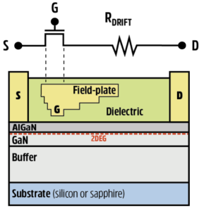
Thanks to the material’s nature, the 2DEG channel at the AlGaN/GaN interface forms spontaneously, with no need for external gate bias. This means the device is normally-on and requires a negative gate bias to deplete the channel and turn it off. It is, in fact, a depletion mode (d-mode) device. Power electronic systems, however, require normally-off devices for fail-safe operations.
The question then becomes how to make the lateral GaN HEMT normally-off. This is where cascode and e-mode (p-GaN gate) technologies part ways.
In the cascode technology, the GaN HEMT is untouched to retain its highest performance and reliability. In its natural state, the 2DEG channel is free to maximize its unparalleled combination of high mobility and charge density. Transphorm’s cascode approach pairs the GaN HEMT with a low-voltage, normally-off Si MOSFET to achieve normally-off operation. This solution provides a positive threshold voltage of 2.5 V to 4.0 V, depending on power level, topology, and system architecture.
Alternatively, an e-mode approach opts to control the 2DEG channel inside the HEMT itself — a design decision that negatively impacts the 2DEG’s advantage.
E-Mode GaN throttles the 2DEG’s natural benefits
When power engineers modify a lateral GaN HEMT to achieve normally-off behavior, critical compromises are made. First, the 2DEG’s charge density must be reduced, which generates a higher resistance per unit area (Figure 2) and a lower figure of merit than achieved in its natural state.
Second, a p-type doped GaN layer (Figure 3) must be added under the gate metal. The p-GaN layer serves as a built-in negative battery (approximately -3.2 V) that turns the 2DEG channel off and yields a barely positive threshold voltage of approximately 1.6 V.
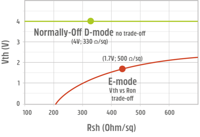

When dealing with noisy environments or high-power levels, a 1.6 V threshold may not be enough. A negative gate drive of approximately -3 V will then likely be used, adding circuit complexity and additional dead-time loss. In fact, with a gate bias of -3 V, the reverse current flowing from source to drain must overcome the negative gate voltage, which causes additional undesired power loss. Notably, the negative drive’s negative impact on the dynamic or switching resistance of the device (which is the relevant resistance in the application) is not taken into account in e-mode device datasheets and is a major topic of study and concern.1
The domino effect: E-Mode’s lack of isolation, dynamic threshold issues, low performance, and fragility
The e-mode modifications indicated above come at a cost: the loss of gate isolation…and more.
Replacing the gate dielectric with p-type GaN results in the gate no longer being isolated. Which, in turn, causes a significant gate current under positive bias, posing severe constraints to maximum gate voltage ratings. To reduce that significant gate current, yet another modification is made: the gate contact is changed from an ohmic metal to a Schottky barrier (Figure 3B).
The Schottky barrier then introduces another challenge as it now hinders the discharge of the gate-drain capacitance during turn-on transient. This, in turn, leads to a detrimental phenomenon referred to as “dynamic threshold” (reported by several research groups2, 3), which causes dynamic on-state resistance issues, as shown in Figure 4. At a voltage of 480 V, an e-mode device shows a dynamic RDS(on) increase of 27%, whereas its cascode counterpart shows only 5% resulting in fewer conduction losses. The e-mode data reported in Figure 4 is consistent with what’s shown in independent research studies.4
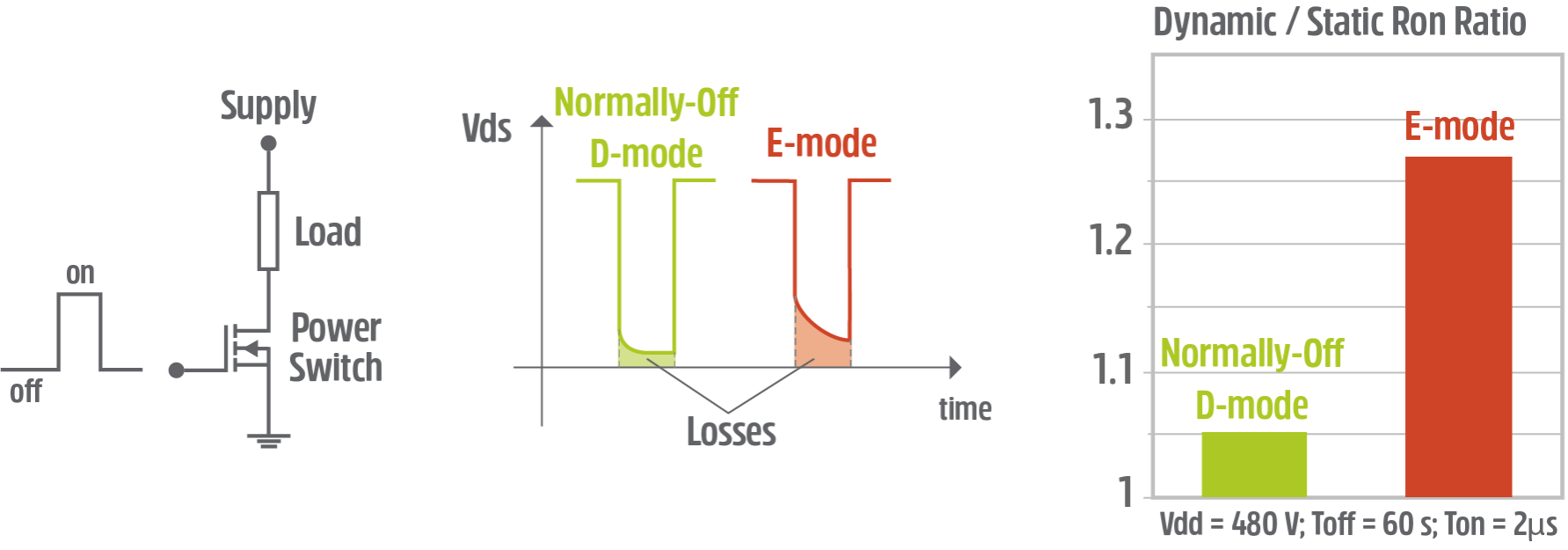
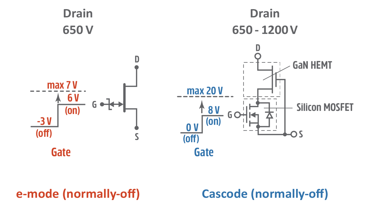
Due to difficulty in discharging the capacitance, the e-mode device’s threshold voltage is now unstable during switching. This results in higher power losses versus its cascode counterpart. (Note: This is likely why e-mode manufacturers do not typically report dynamic RDS(on) ratings.) To mitigate this problem, one could theoretically overdrive the gate to reduce the RDS(on) of the device under the gate. However, this potential solution is up against a very tight voltage window as it must comply with a small gate maximum rating to prevent gate damage (max 7 V) (Figure 5).
Additionally, as the temperature rises during normal device operations, the 2DEG mobility naturally decreases.
The reduction in 2DEG mobility over temperature also causes the p-GaN gate transconductance to drop (Figure 6), resulting in even slower transitions and still more switching losses5 versus that of cascode GaN. The decrease creates the perfect storm for low efficiency. To manage these issues, a p-GaN gate solution would need to start with a larger die which still presents the problem of increased Miller capacitances reducing overall efficiency and higher cost.

Per datasheet ratings, the e-mode device’s on-state resistance shows a higher temperature coefficient than cascode. In fact, it’s as high as 2.6x between 25°C and 150°C (Figure 7), yielding a rapid increase of conduction losses.
The e-mode design constraints continue with the susceptibility of threshold voltage drift due to trap injection into the buffer. e-mode’s silicon substrate must connect to the source terminal to mitigate buffer charging caused by electron injections from the source itself.
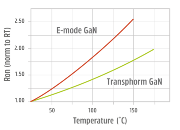
This modification restricts e-mode’s drain voltage maximum rating to 650 V. Given that higher voltages require thicker GaN buffers to support the substrate-to-source connection, e-mode devices are essentially left behind in the race to 1200 V as thicker GaN buffers require more sophisticated technology…which adds still more cost.
The cascode philosophy: the right approach for the right purpose
Transphorm approaches GaN power semiconductors differently. Again, its platform pairs the normally-on GaN HEMT with a highly reliable, highly performant normally-off low-voltage Si MOSFET in a cascode configuration. This ensures the platform’s fail-safe normally-off operations while retaining the highest GaN performance and highest Si MOSFET gate reliability.
Developing a cascode GaN platform was deliberate for various reasons, the most important two being that it works synergistically with nature and is backward compatible with today’s silicon technology. As stated earlier, it allows platform elements—particularly the 2DEG—to do what they do best. So, instead of limiting GaN’s advantages via e-mode (p-GaN gates), cascode embraces GaN’s potential. And the resulting cascode platform stands as a high-performing, highly robust GaN technology with industry-leading reliability and versatility.
Leveraging D-Mode’s natural advantages
Cascode devices do not face the aforementioned challenges experienced by e-mode devices. For example, the cascode solution is unaffected by dynamic threshold issues since one drives a gate-isolated low-voltage Si MOSFET. The threshold voltage is set by the Si MOSFET independent of the GaN HEMT.
The normally off cascode d-mode configuration also generates a second gift from nature in addition to the 2DEG: the SiO2/Si interface. This interface naturally isolates the device gate, offering the automotive-grade maximum gate rating of +/- 20 V with exceptional reliability and a high drive margin. The threshold voltage is as high as 4 V, with no compromises on the 2DEG. The low-voltage Si MOSFET does not require negative bias or any special gate drivers. It is stable under all switching conditions, with no hidden power loss associated with dynamic threshold issues. As can be seen in Figure 6B, the transconductance of cascode GaN devices is exceptionally high and doesn’t drop with temperature because it is set by the Si MOSFET and independent from the 2DEG mobility.
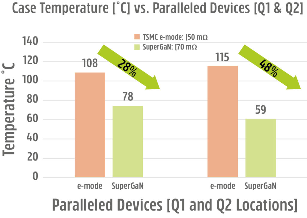
These advantages are backed by real-world data. When Transphorm’s SuperGaN® cascode devices replaced the original e-mode GaN devices shipped in a commercially available power adapter, the SuperGaN FETs delivered higher efficiency and up to 50% lower case temperature despite having a smaller chip size and a 30% higher on-resistance rating (Figure 8).
GaN package versatility equals customer application compatibility
The normally-off cascode platform fits elegantly in a broad range of standard packages such as through-holes, surface mounts, and multi-chip modules. These packages are considered high-performing and highly reliable in their own right, adding to the performance and reliability of the GaN platform itself.
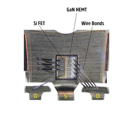
With modern assembly and packaging technologies, the parasitic inductances of Transphorm’s high-power cascode products are minimized. In fact, Transphorm’s SuperGaN normally-off cascode platform features a die-on-die technology with silicon-like wire bonding (Figure 9). No additional wire bonds or parasitic inductance are added, which allows for the desired connection scheme, including wire bond, copper clip, and Kelvin source.
The cascode configuration also lends itself beautifully to system-in-package integration, where the gate driver and controller are integrated seamlessly with the d-mode HEMT and low-voltage Si MOSFET (monolithically or hybrid) — adding still another option to satisfy diverse end application requirements.
Additional considerations
The cascode d-mode GaN HEMT does not need to connect the source to the substrate. A floating or insulating substrate enables a higher voltage rating (ex: up to 1200 V7) and bidirectional switch implementation.8
Interestingly, if one wants to develop a bidirectional switch using p-GaN gates, they will face yet another difficult decision: As both terminals alternate their polarity from ground to DC bus voltage, which terminal should the substrate connect to? It’s a question with no clear answer.
Cascode d-mode GaN HEMTs deliver one more critical advantage not readily accessible to e-mode HEMTs today
As GaN transistors penetrate the motor drive market, short-circuit capability will be required. d-mode’s insulated gate voltage handling allows for very elegant design methods. Such methods are proven to tailor the short-circuit withstand time (SCWT) of Transphorm’s d-mode devices up to 5 microseconds,9 meeting the requirements of commercially available gate drivers. Transphorm achieves SCWT through its proprietary semiconductor process without adding additional masks or current sensing pins — making three-leaded packages still applicable. To date, e-mode does not seem fully prepared for this eventuality, with demonstrations being limited and sometimes misleading.
Conclusion
When considering the above-listed advantages and others, the normally-off cascode d-mode platform generates a portfolio of GaN devices that optimize and magnify the inherent advantages of GaN as a semiconductor material — producing a truly revolutionary power conversion solution for next-generation power electronics.
Myth busting
Myth #1: Si MOSFETs add-on state resistance reverse recovery charge
Uncover what chip really handles the majority of off-state high voltage — and which one contributes less than 10 percent of the total cascode resistance.
Myth #2: e-mode devices have no Qrr
Yes, GaN HEMTs have no reverse conduction bipolar transport, but completely eliminating Qrr? Think again.
Myth #3: Cascode GaN oscillates
Read how following standard design principles enhances performance and suppresses oscillations and EMI.
Endnotes
1 J. Wei et al., “Dynamic Threshold Voltage in p-GaN Gate HEMT,” 2019 31st International Symposium on Power Semiconductor Devices and ICs (ISPSD), Shanghai, China, 2019, pp. 291-294, doi: 10.1109/ISPSD.2019.8757602.
2 Ibid.
3 A. Chini et al., “Gate-Bias Induced RON Instability in p-GaN Power HEMTs,” in IEEE Electron Device Letters, vol. 44, no. 6, pp. 915-918, June 2023, doi: 10.1109/LED.2023.3265503.
4 Zhong et al., “IG- and VGS-Dependent Dynamic RON Characterization of Commercial High-Voltage p-GaN Gate Power HEMTs” Digital Object Identifier 10.1109/TIE.2021.3104592.
5 S. I. H. Sabzevari, S. Abdi and R. Ghazi, “Assessment of the Switching Characteristics of a commercial e-mode Power GaN Device Using a Dual Pulse Test Set-up,” 2021 IEEE 15th International Conference on Compatibility, Power Electronics and Power Engineering (CPE-POWERENG), Florence, Italy, 2021, pp. 1-6, doi: 10.1109/CPE-POWERENG50821.2021.9501072.
6 Recommended External Circuitry for Transphorm GaN FETs (Application Note No. 0009). Retrieved from Transphorm Inc. website: https://www.transphormusa.com/en/document/recommended-external-circuitry-transphorm-gan-fets/.
7 G. Gupta et al., “1200V GaN Switches on Sapphire Substrate,” 2022 IEEE 34th International Symposium on Power Semiconductor Devices and ICs (ISPSD), Vancouver, BC, Canada, 2022, 349-352, doi: 10.1109/ISPSD49238.2022.9813640.
8 J. Huber and J. W. Kolar, “Monolithic Bidirectional Power Transistors,” in IEEE Power Electronics Magazine, vol. 10, no. 1, pp. 28-38, March 2023, doi: 10.1109/MPEL.2023.3234747.
9 D. Bisi et al., “Short-Circuit Capability with GaN HEMTs: Invited,” 2022 IEEE International Reliability Physics Symposium (IRPS), Dallas, TX, USA, 2022, pp. 1-7, doi: 10.1109/ IRPS48227.2022.9764492.



I learned about this article when reading an email from power electronic tips and in that email they commended this article and touting this is “The editor’s choice” article and in that email they pinned figure 8 as it’s face. I suppose it doesn’t matter, or hardly matters, as I personally would love to see how the authors determined that a drop of thirty degrees celsius is equivalent to a thirty one percent reduction in temperature. Actually, I’m not interested in that but wondering how in this day and age we’re still producing charts that are implying that heat can be reduced beyond 100%.
This marketing faupa inspires no confidence and compells me to question the validity of all the other claims in the article. But not just this article, the others shared in that email are called into question as well. I don’t have the time to evaluate all these for additional elementary errors. Fix it and be more careful next time. The reductions are 7.87% and 14.43% heat respectively.