
Gate drivers hold the key for efficient wide bandgap semiconductor adoption on the road to sustainability.
Innovative companies are developing disruptive new technologies that move the world towards a safer and more sustainable future. Wide bandgap semiconductors, notably GaN and SiC transistors, are a present-day example of a rapidly emerging and disruptive technology that dramatically improves power electronics systems’ size, weight, and efficiency.
Both GaN-based and SiC-based transistors have lower gate capacitance and can, therefore, switch much faster than silicon-based alternatives. Power system designers can increase the switching frequency of wide bandgap transistors, thereby enabling smaller inductor sizes and reduced switching losses (higher efficiency) in power electronic systems. Additionally, wide bandgap devices can often operate at higher temperatures than silicon alternatives, enabling higher operating currents and/or reducing the size and cost of heat-sinking elements in power electronic systems.
As a result of these benefits, wide bandgap semiconductor devices are disrupting the power electronics industry. GaN and SiC technology underpin a more sustainable future with longer-range electric cars, higher-efficiency solar energy systems, and high-efficiency power supplies that reduce the electricity consumption of advanced and continuously operating data centers.
There is clear evidence that battery electric vehicles are adopting GaN technologies for their onboard chargers. Using GaN in such chargers reduces system size and weight, helping to improve the driving range and charging cost of electric vehicles. In the age of commuters seeking ever-increased EV range and lower charging costs and OEMs determined to deliver the features that car owners seek, these benefits are a big boost for business.
Enter highly integrated gate drivers
A technical challenge concerns using SiC and GaN in power electronics systems. Compared to silicon transistors, wide bandgap devices are often harder to drive, control, and protect during normal operation and transient or short-circuit events. In many ways, system designers must trade off the complexity of driving SiC and GaN transistors to reap wide- bandgap transistors’ efficiency, size, and weight benefits offered by a wide bandgap transistors.
If a short circuit event were to occur, a quick reaction time is essential to protect any component and system from catastrophe if a short circuit event occurs. GaN devices must be turned off incredibly quickly — within 0.1 µs — to protect the devices from damage. High-speed current sensors are often used to rapidly detect these types of short-circuit events. When Allegro’s isolated gate drivers are coupled with high-speed current sensors, the safety of designers’ systems is assured. Allegro’s high-speed, lossless current sensor ICs reduce ohmic losses in a power electronics system and offer robust and accurate system control. These small form factor current sensor ICs include an integrated overcurrent comparator that responds to an overcurrent event in as little as 65 ns. This high-speed overcurrent detection feature helps systems designers protect transistors from overcurrent events, offering a substantial risk mitigation benefit.
A typical gate driver design for a >400 V system uses 2 IC packages (an isolated gate driver and an isolated power supply), a transformer (discrete or integrated), and several passive discrete components. These components use valuable printed circuit board (PCB) space, and designers must contend with the interconnect’s reliability and performance impact. These are conditions in which parasitic power loss is all but guaranteed, forcing engineers to try to compensate for the losses in various ways. This 2-chip solution is also far less efficient than it could be, as power density also suffers, so any power delivered to its destination may see a significant decrease from what designers envision and initially expect to occur. However, driving GaN and SiC transistors is becoming easier with the release of new, innovative, highly integrated isolated gate driver ICs, simplifying designs with smaller footprints and higher efficiency.
Gain a better perspective with GaN
Integrating various active and magnetic components in a single semiconductor- grade package can minimize PCB space and interconnects, significantly reducing overall package size and increasing efficiency. With a much smaller footprint, GaN-based gate drivers are much more power-dense, which signals substantial present and future benefits for designers using them.
Recent developments in the electric vehicle industry demonstrate the benefits of a switch to GaN solutions, particularly in the onboard charger market. In one instance, a European charger OEM has delivered a notably smaller charging solution by opting for a GaN-based device, shrinking their onboard charger from approximately 30 Liters to 16 Liters. This significant volume reduction is associated with lower overall curb weight, which delivers better overall vehicular range. This feature is not only of increasing consumer demand but overall importance as EVs become more commonplace.
Challenges meet solutions
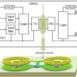
Companies developing disruptive, single-package, isolated gate driver ICs (with integrated inductor and DC/DC converter) that solves previously noted problems. These ICs boasts a small form factor, high power density, low common mode capacitance, and much lower Electromagnetic Interference (EMI) than typical drivers. Primary-to-secondary coupling capacitance of many isolated gate driver designs poses a significant challenge for wide bandgap power switches as they switch much faster than silicon power devices. Faster switching transitions create much higher dv/dt and increase common mode current transients, requiring additional efforts for EMI mitigation. The primary-to-secondary capacitance must be charged and discharged at each switching instance, and the power loss is directly proportional to the switching frequency. Reducing the capacitance between primary and secondary can reduce power losses and simplify EMI mitigation.

Many common gate drivers have a primary-to-secondary capacitance of 8–10 pF or higher. However, with patented Power-Thru technology, Allegro’s gate drivers reduce the primary-to-secondary capacitance to less than 1 pF, reducing power losses and simplifying EMI compliance efforts. In a typical application, Power-Thru allows gate drivers to reduce power loss by more than 1 W per power switch and noise injection by more than 20 dB. In addition to its strong power and efficiency benefits, using fewer external discrete components in the AHV85110 leads to additional area savings at the PCB level. Allegro’s highly integrated IC requires less than six external components, compared to 15 to 20 external components required when using competitor multi-chip devices.

The increase in system efficiency, reduction in used PCB area, and lower overall volume associated with innovative, highly integrated gate driver ICs can be substantial compared to multi-chip solutions. For example, a 22 kW onboard charger design using GaN transistors may require up to 32 isolated gate driver ICs and isolated DC/DC converters. A single-chip isolated gate driver IC using a single transformer for both the isolated voltage converter and isolated gate drive functions can reduce power loss between components.
In the case of the aforementioned 22 kW charger, highly integrated gate driver solutions offer demonstrable, significant efficiency benefits and space savings of 32x relative to conventional dual-chip ICs, which typically require 5 to 15 more external passive components.
Engineers in the automotive industry have expressed a strong belief that GaN drivers will be more broadly adopted soon. Additionally, many of the same engineers have indicated that the innovative, efficient, small form factor isolated gate drivers like the AHV85110 and AHV85111 may shape the future roadmap of power electronics systems in electric vehicles. With many applications and benefits, forward-thinking system designers in clean energy, data centers, and xEV markets should strongly consider incorporating isolated gate drivers into their designs.
Leave a Reply