
Outer space is harsh, but it’s relatively kind to gallium-nitride (GaN) power transistors compared with their Si (Si) counterparts. Si devices require special processing for protection against the total ionizing dose (TID) impact of exposure to radiation in space. GaN has material properties and construction advantages that make it less subject to damage caused by TID. But, to withstand the detrimental effects of single event effects (SEE), GaN and Si both need special processing. In addition to high radiation levels, there are very low temperatures in space, and the cryogenic environment can impact power transistor performance.
This FAQ first reviews aspects of GaN power transistor operation when exposed to gamma radiation, proton, neutron radiation, or heavy ion bombardment. It then looks at the CREME96 tool for creating numerical models of the ionizing-radiation environment in near-Earth orbits then considers the impact of cryogenic temperatures on GaN operation. It closes with an overview of the benefits of using GaN-based power converters in spacecraft.
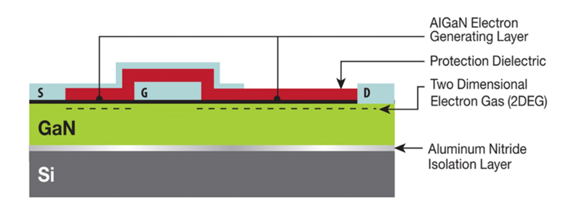
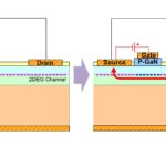
The lateral structure of enhancement-mode (e-mode) GaN devices is an important factor in their superior radiation tolerance compared with the vertical structure of Si MOSFETs (Figure 1). An e-mode GaN device has an aluminum gallium nitride (AlGaN) layer between the gate and the two-dimensional electron gas (2DEG) conducting layer. When subjected to gamma radiation, the AlGaN layer doesn’t accumulate charge and does not suffer from the ‘charge trapping’ effect that hinders the performance of Si MOSFETs.
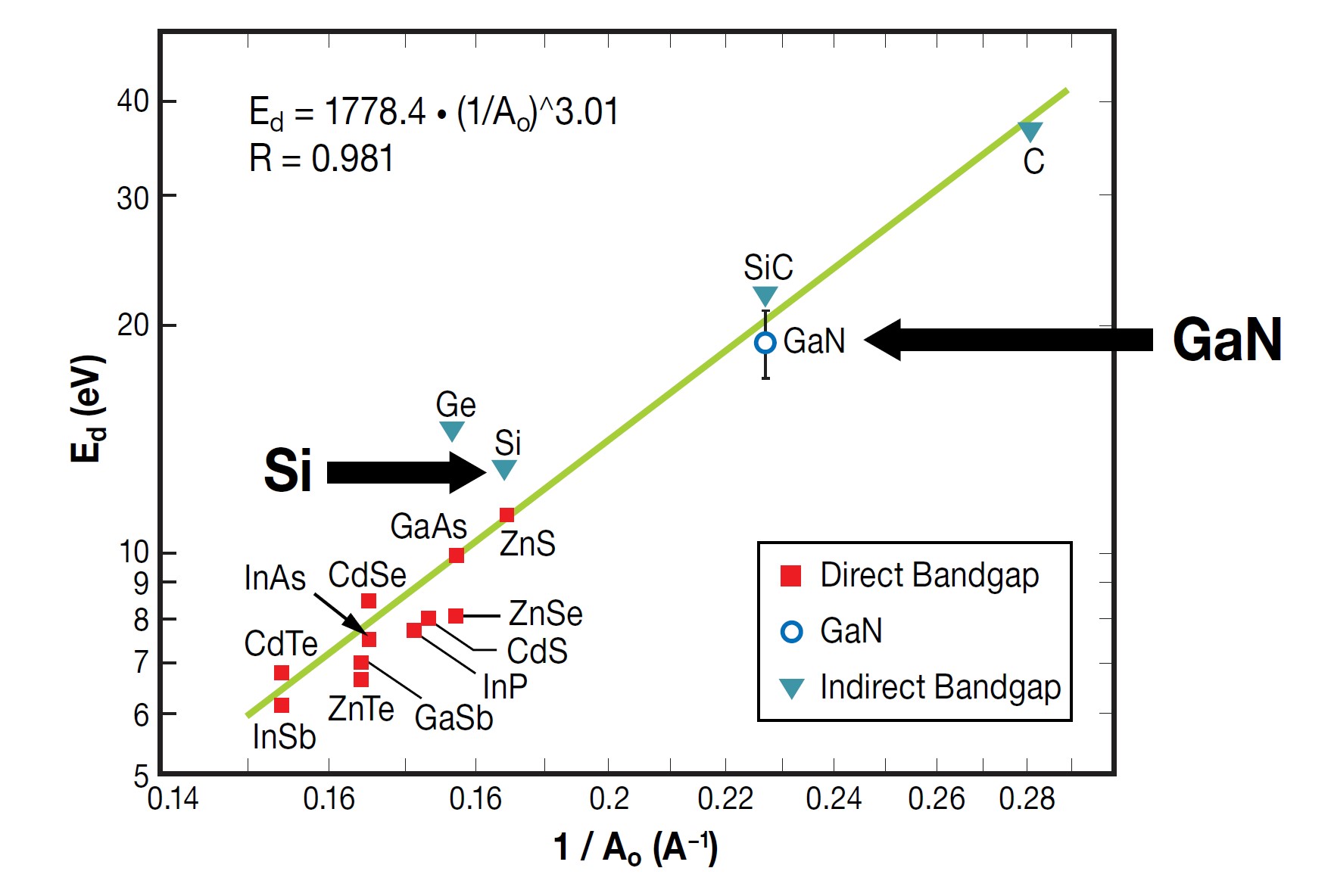
Energetic protons can interact with GaN’s crystal lattice, causing increased defect densities. More defects reduce mobility with a corresponding increase of on resistance, an increase in threshold voltage, and a reduction in the peak transconductance value and the saturation current. In general, these effects appear to be small, with minimal impact on device performance. Neutron radiation has a similar effect on performance, increasing the threshold voltage and decreasing material mobility. GaN’s higher displacement threshold energy than Si results in better performance than Si devices (Figure 2).
Heavy Ion Bombardment (SEE)
Highly-energetic heavy ions, protons, and neutrons are the source of single-event effects (SEE). The structure of e-mode GaN devices makes them much less susceptible to SEE compared with Si MOSFETs. The lack of a gate oxide in GaN devices means that single event gate rupture (SEGR) cannot happen. The lack of parasitic bipolar junctions found in Si MOSFETs, means that single event upset (SEU) or single event burnout (SEB) do not happen in GaN devices. However, heavy-ion bombardment of GaN devices can degrade the drain-source leakage. With the proper design and processing techniques, GaN devices can be fabricated that are immune to SEE.
CREME96 for evaluating radiation levels
The Cosmic Ray on Micro-Electronics evaluation code (CREME96) is often used for modeling the impact of ionizing radiation in low earth orbits. The CREME96 program uses a linear energy transfer (LET) spectrum as the input for calculating the rates of SEEs. The CREME96 program can produce a graph of the integral flux (measured in particles/m2-s-sr) versus the LET (measured in Mev•cm2/g) (Figure 3). The flux of particles for a given LET is shown as colored lines in the graph.
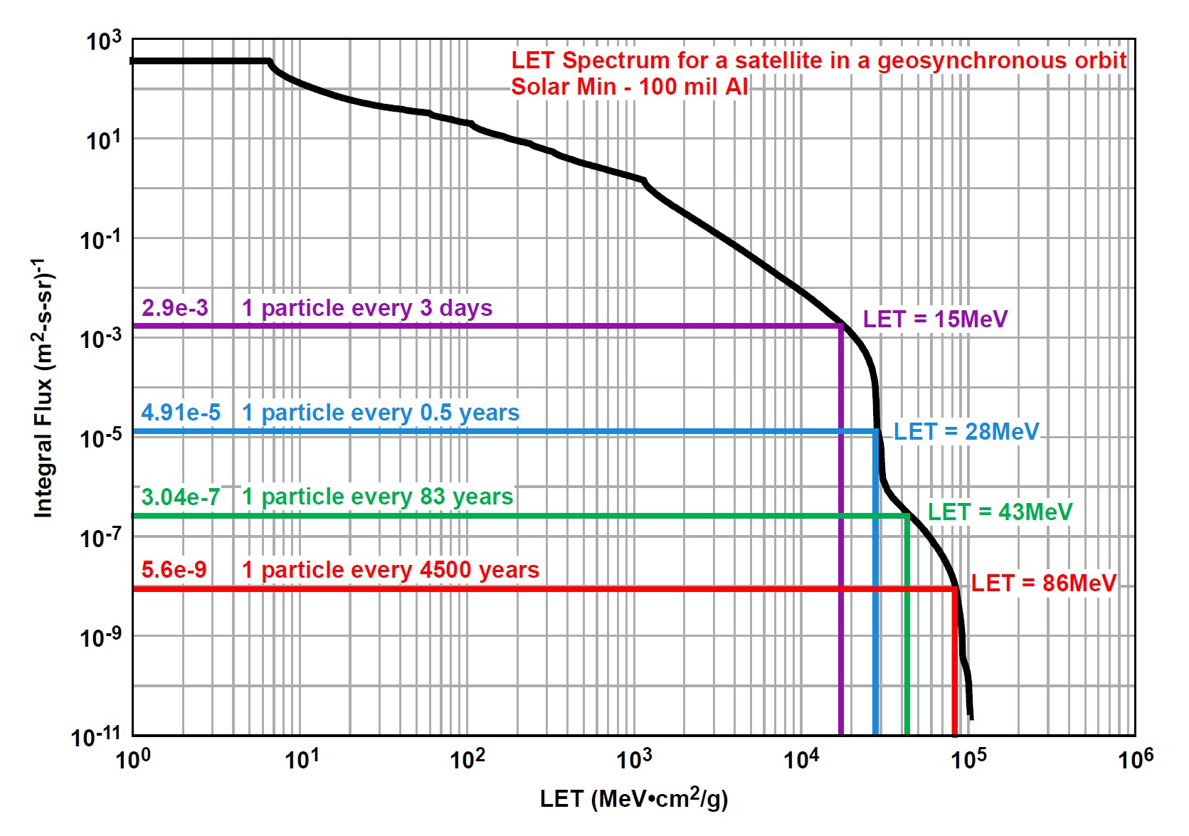
The particle fluence (total number of particles over a given period of time) can be used to determine the long-term mission impact of radiation. A typical e-mode GaN device can withstand energy of 43MeV with a minimal performance impact. Referring to the green line in the graph above, a GaN device in a satellite would see a particle with an LET of ≥ 43MeV approximately once every 83 years in a geosynchronous orbit. An energy level of ≥ 86MeV (the red line) can result in a hard fault in a GaN device which can be catastrophic to the system, but its statistical likelihood is very low (once in 4,500 years).
SEE testing of 40V, 100V, and 200V GaN FETs identified a current increase at energies above 43Mev•cm2/mg and higher supply voltages. However, the low fluence of ions in geosynchronous orbit with these high energies means that the actual increase in current during a 20-year mission is expected to be very small.
Space can be cryogenic
While GaN has an inherently higher displacement threshold energy resulting in superior performance under neutron radiation than Si and most other materials, operation in cryogenic environments, such as space, depends on the specific device structure. Si, Si-carbide, and emerging vertical GaN devices employ doping of the semiconductor materials and exhibit two main effects at low operating temperatures. First, there’s an increase in carrier mobility, enhancing performance. Second, a freeze-out of dopants decreases carrier density, increasing the threshold voltage and the channel resistance. Lateral e-mode GaN devices don’t use doping; the carriers are generated due to the polarization mismatch between the GaN and AlGaN layers. As a result, lateral GaN devices have improved carrier mobility at low temperatures but do not experience freeze-out. In a recent study, a cryogenic probe station was used to measure the different loss contributions (conduction, hard- and soft- switching) as well as the device gate control as a function of temperature for four GaN commercial power devices in the temperature range between 400 K and 4.2 K (Figure 4).
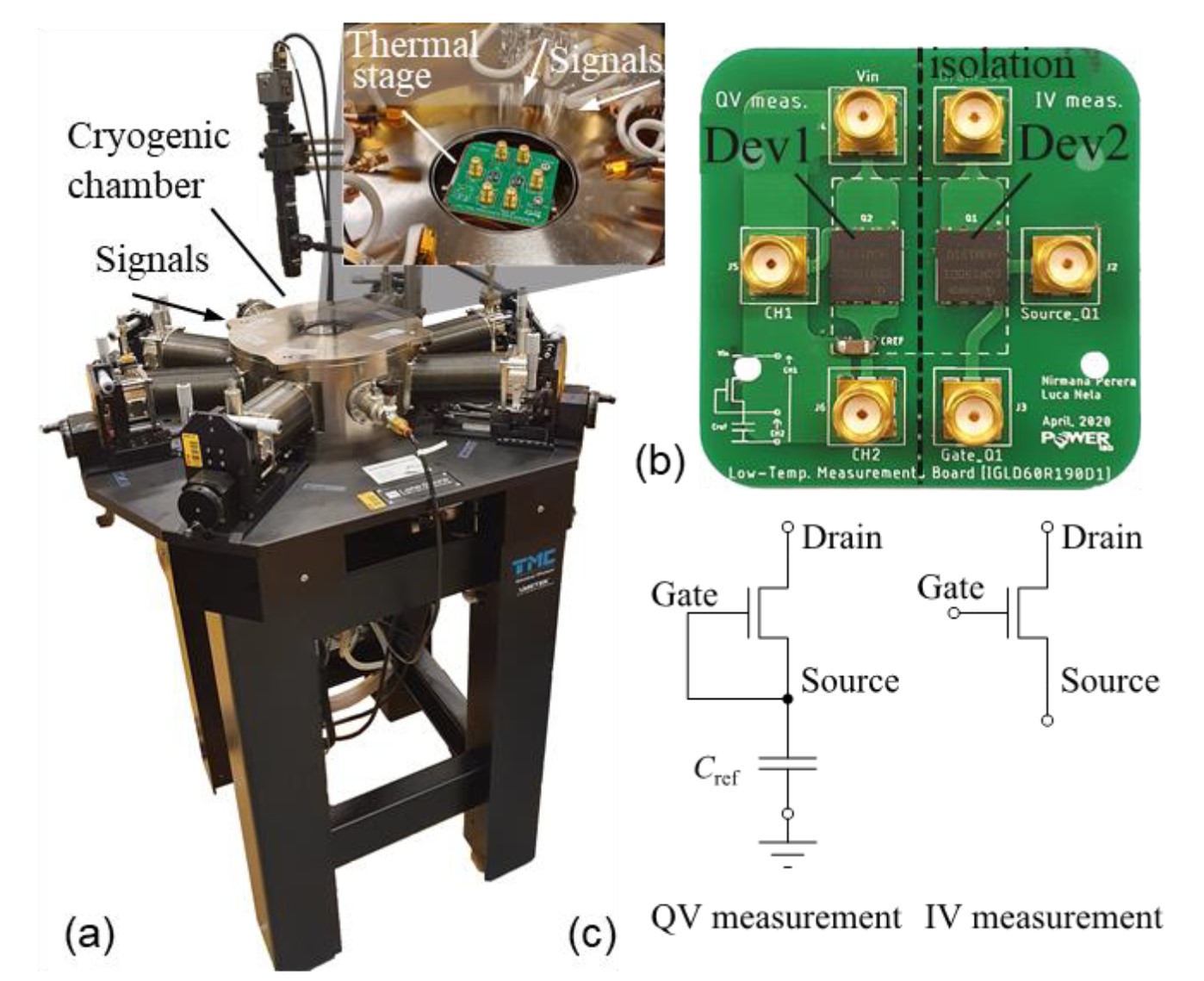
The tests included a Schottky p-GaN device (T1), Cascode device (T2), and two Ohmic p-GaN (GIT) devices (T3 and T4). A comparison was made of RON, the energy dissipated at each switching cycle (EDiss), and the energy stored in the transistor output capacitance (Eoss) at 400 K and 4.2 K. (Table 1). As a result of increased electron mobility, all devices demonstrated a significant RON reduction at a lower temperature. The actual amount of the change is dependent on the device structure. The most significant decrease was in conduction losses, about 6X for T1 and T2 and about 2X for T3 and T4. Conduction losses show the most significant decrease, which is larger (about 6x) for conventional HEMT technologies (T1 and T2) with respect to the GIT devices (about 2x). For soft-switching and hard-switching losses, there was more variability between the devices. All the GaN power devices show enhanced efficiency at cryogenic temperatures, with the level of improvement dependent on device structure and circuit operation.

The bottom line – Power converter performance
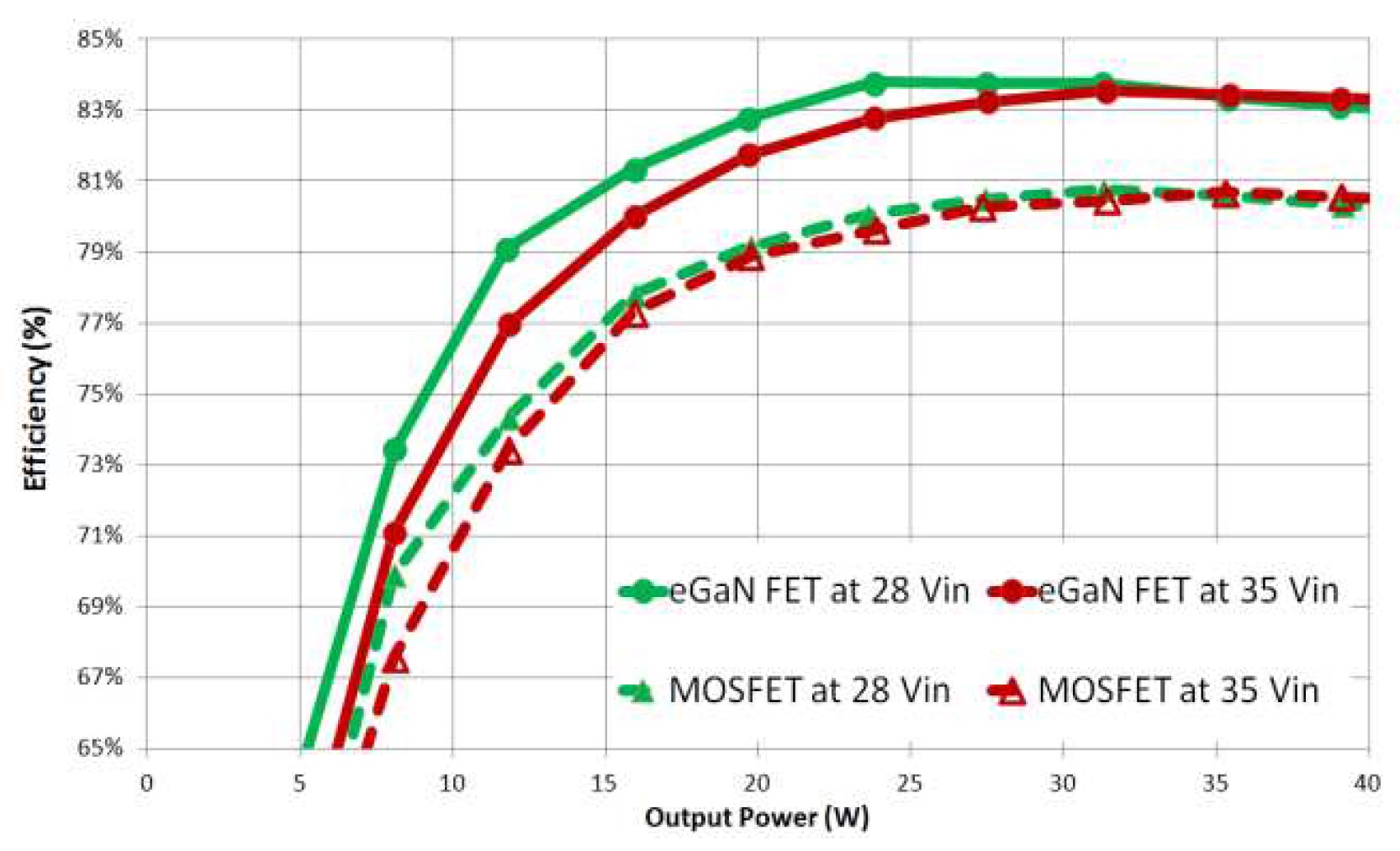
Si power MOSFETs have lower performance to achieve radiation tolerance, leading to space-qualified power converters with lower efficiencies than their commercial equivalents. GaN power devices do not suffer from the performance trade-offs inherent in Si MOSFETs. In one comparison using a dual output 50W clamped forward converter, the radiation-tolerant power MOSFETs in the original design were replaced with e-mode GaN FETs. In addition, an LM5114 driver IC was added to act as a buffer between the control circuit designed for the Si MOSFET and the GaN device.
This dc/dc converter was designed to operate from a 28V power bus and rated 100 kRad(Si) with a SEE rating of more than 80 Mev•cm2/mg. Simply by replacing the radiation-tolerant power MOSFETs with GaN devices, efficiency increased (Figure 5). In a new design based on e-mode GaN devices, a higher switching frequency can be used, leading to smaller passive devices (magnetics, inductors, and capacitors), a further reduction in converter size and weight, and significantly greater power density, with no thermal penalty.
Summary
Compared with Si MOSFETs, e-mode GaN FETs demonstrate superior performance in high radiation environments found in near-earth and geosynchronous orbits. The material properties of GaN, including its higher displacement threshold energy, are the primary sources of its superior performance under neutron radiation compared with Si and other materials. The device structure, including the lack of doping, is the major contributor to GaN’s superior operation in cryogenic environments, such as space. Finally, e-mode GaN FETs have demonstrated their ability to withstand harsh radiation and cryogenic environments while still delivering increased power converter efficiencies compared with radiation-tolerant Si MOSFETs.
References
Considerations for GaN power devices for low-temperature operation and Space Applications, Teledyne Hirel Electronics
CREME96: A Revision of the Cosmic Ray Effects on Micro-Electronics Code, IEEE Transactions on Nuclear Science
GaN FET Current Increase Due to Heavy Ion Testing, Renesas
Impact of Gamma Radiation on Dynamic R DSON Characteristics in AlGaN/GaN Power HEMTs, National Library of Medicine
Performance of GaN Power Devices for Cryogenic Applications down to 4.2 K, IEEE Transactions on Power Electronics
Radiation Performance of Enhancement-Mode Gallium Nitride Power Devices, EPC Space
Radiation Tolerant Enhancement Mode Gallium Nitride (eGaN®) FETs in DC-DC Converters, EPC
The Study of the Single Event Effect in AlGaN/GaN HEMT Based on a Cascode Structure, MDPI electronics
What is Radiation-Hardened Gallium Nitride?, EPC Space
Leave a Reply