Gallium-nitride (GaN) power semiconductors are well-established, but compared with silicon (Si) devices, GaN is still an evolving power device technology. Most power designers have at least explored the use of GaN, whether it’s been depletion-mode (d-GaN) normally-on devices, enhancement-mode (e-GaN) normally-off devices, a cascode combination of a Si MOSFET with a d-GaN device to form a normally-off structure, or a GaN power IC. Those options continue to advance. More recently, high-voltage vertical GaN (v-GaN) devices have entered the commercial arena.
This FAQ looks briefly at GaN HEMT physics, reviews the performance and tradeoffs between lateral d-GaN, and e-GaN, looks at integrated GaN solutions that can simplify power converter designs, and closes by presenting the emerging v-GaN technology.
GaN has the widest energy gap, the largest critical field, and the highest saturation velocity of commonly-used semiconductor materials. In addition, spontaneous piezoelectric polarization of AlGaN/GaN heterostructures creates a two-dimensional electron gas (2DEG), with high mobility and large channel density, without the use of doping. These factors contribute to minimal on resistance (RON), and the structure of lateral GaN devices has very small parasitic capacitance and switching charges enabling very high-frequency operation.
GaN is a wide bandgap (WBG) material and has a bandgap of 3.4 electron volts (eV) compared with 1.12 eV for Si and 3.2 eV for 4H-SiC (Figure 1). Its wide bandgap enables GaN to be operated at higher temperatures, increasing the potential power density of converters using GaN HEMTs. GaN has a thermal conductivity of 2.0 W/cmK, intermediate between Si with thermal conductivity of 1.5 W/cmK, and 4H-SiC with 4.9 W/cmK.
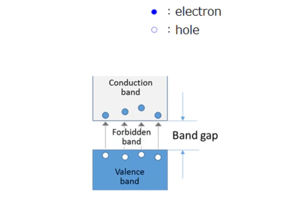
GaN’s high breakdown field of 3.3 MV/cm is 11 times higher than Si with 0.3 MV/cm. That means that a layer of GaN can be 11 times thinner than Si and still withstand the same voltage, and the GaN layer will have a lower resistivity contributing to lower RON. GaN’s high channel mobility (up to 2000 cm2/V s) and large saturation velocity (2.5 × 107 cm/s) also contribute to lower RON.
Lateral d-GaN and e-Gan
In lateral GaN HEMTs, the gate, source, and drain are all on top with the gate sitting on the AlGaN layer, and the source and drain electrodes piercing through the AlGaN layer to form an ohmic contact with the underlying 2DEG, which is where current flow occurs (Figure 2). In both d-mode and e-mode HEMTs, higher voltage devices have a greater separation between the drain and gate. D-mode GaN devices are normally ON, and current flows between the drain and source with no potential applied to the gate. When using d-GaN devices, the switch must be turned OFF before turning the power converter to avoid a short circuit at startup. D-mode GaN HEMTs are not used as stand-alone switches in power conversion applications.
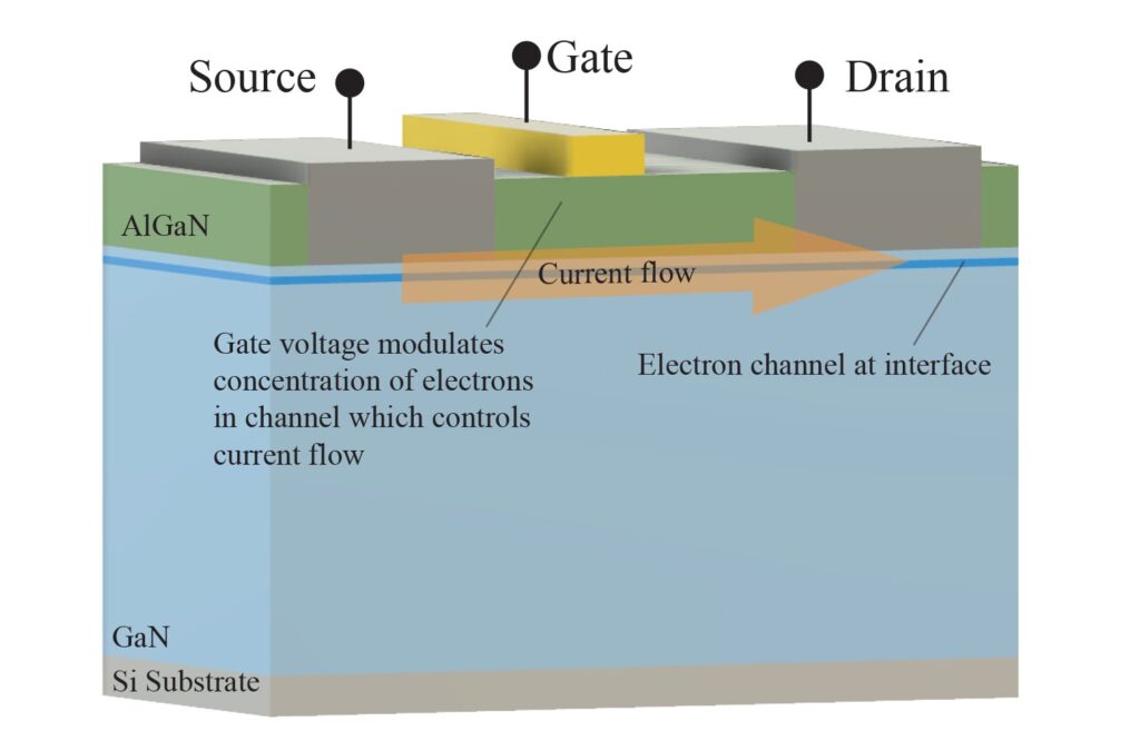
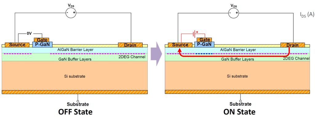
GaN HEMTs used in power converters are required to be normally-off devices to ensure safe operation: If the gate driver is off or fails and its output is zero, the HEMT must turn OFF. That’s not possible without modifying the d-mode GaN structure. Two common solutions are:
- Placing a p-GaN or p-AlGaN layer between the gate and the AlGaN/GaN heterostructure. The p-type layer effectively depletes the 2DEG with VGS = 0, resulting in a normally-off device. This approach is called e-GaN (Figure 3).
- The use of a cascode pair of devices, including a d-GaN HEMT and a low-voltage Si MOSFET. There are advantages to using the Si MOSFET to turn the combined device ON and OFF, while the GaN HEMT provides high-voltage and low RON operation.
Cascode GaN
A cascode structure copackages a high-voltage d-GaN HEMT (for example, 600V) and low-voltage Si MOSFET (usually a 30V device) to achieve enhancement mode operation (Figure 4). The Si MOSFET is used to switch the GaN HEMT on and off with minimal increases in RON or reverse recovery charge (QRR). Combining a 600V GaN device with a Si MOSFET will have less than a 5 percent increase in RON compared with the GaN device alone. The increase in QRR is even lower, with the combined structure having a QRR about an order of magnitude lower than a high-voltage Si MOSFET with ratings equal to the high-voltage HEMT.
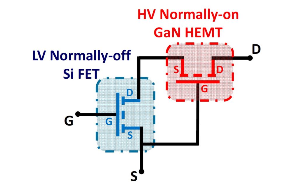
Cascode devices have efficiencies and thermal characteristics similar to e-GaN devices. But, the cascode structure has the robust and reliable silicon dielectric gate structure, with an effective gate rating as high as ± 20 V, making it compatible with standard, low-cost gate driver ICs.
Cascode devices are often used in high-voltage, high-current, and high-power applications such as automotive systems. Using an AEC-Q101-qualified Si MOSFET can simplify the automotive qualification of cascode devices. A relatively high 4V threshold voltage minimizes the possibility of accidental turn ON due to high dv/dt or di/dt, and minimizes shoot-through risks.
Integrated GaN solutions
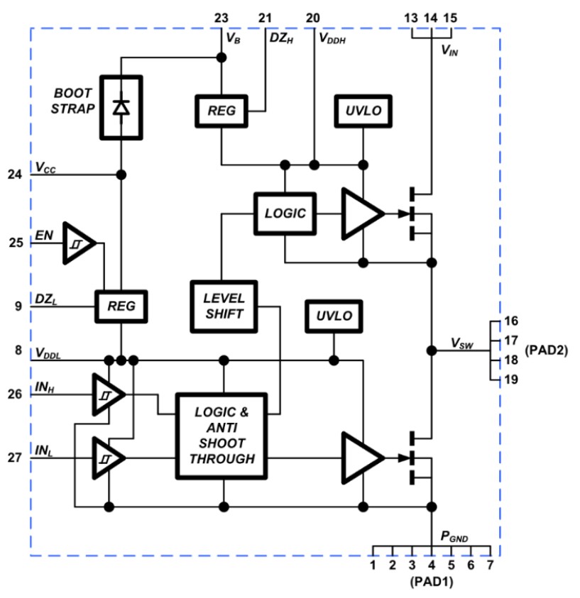
Integrated GaN solutions range from two GaN devices in a half-bridge topology in the same package to complete solutions including drivers, controllers, and other functions. How important is GaN integration? It appears to be very important: According to independent reports, the top two GaN suppliers in terms of the market share at the time of this writing offer highly integrated GaN solutions. For example, a GaN 600V integrated half-bridge IC is available with (Figure 5):
- High-side and low-side GaN FETs and drivers
- Gate voltage regulation
- Hysteretic digital inputs compatible with analog and digital controllers
- Integrated high voltage FET for fast bootstrap capacitor charging to support high-frequency operation
- Low loss and fast level-shift circuit with >200V/ns common-mode noise immunity
- UVLO for safe startup and shut down
- ESD protection
- Shoot-through protection
- Chip enable function for low loss standby mode operation
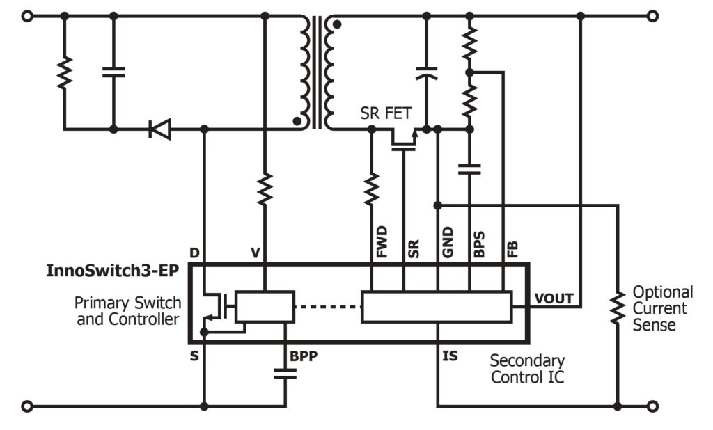
Another integrated GaN power IC can design off-line flyback converters with synchronous rectification (Figure 6). This IC can be used to implement constant or constant current quasi-resonant converters. Depending on the model, it includes a 725 V, 750 V, or 900 V GaN primary switch. These power ICs include both primary and secondary controllers, sense elements, and a safety-rated feedback link from the secondary to the primary side. They can be used to design multiple-output converters with good cross-regulation and include a host of protection features. They are targeted at power converters up to 45 W and have a no load power consumption under 15 mW to satisfy global efficiency standards.
v-GaN for high voltages
While today’s GaN FETs employ lateral structures, most silicon (Si) and silicon-carbide (SiC) power devices use vertical structures that employ impurity doping to fabricate the device. Lateral GaN FETs are fabricated on Si wafers that are inexpensive and are available in large formats, helping to minimize the cost of d-GaN and e-GaN devices. A drawback to growing GaN on Si is an increase in crystal defects in the GaN layer, which can be 108 cm-2, or greater. The defects reduce the high voltage capability of the devices, limiting lateral GaN devices to 900V or less. In the largest number of mains- or battery-powered applications, devices rated for 900V or less are adequate, and lateral GaN devices address a very large market. For higher-voltage applications, Si and SiC devices are currently used. Emerging v-GaN technology is aimed at applications that need devices rated for 1kV and higher, currently using Si and SiC.
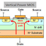
v-GaN devices require a bulk GaN substrate (Figure 7). Since the drift region and substrate are both GaN, defect densities need to be much lower than lateral GaN grown on Si substrates. Defect densities in v-GaN structures will be about 103 to 105 cm-2, 1,000 to 10,000 times less than lateral structures. The low defect density of v-GaN device structures will translate into voltage ratings up to 10kV or higher.
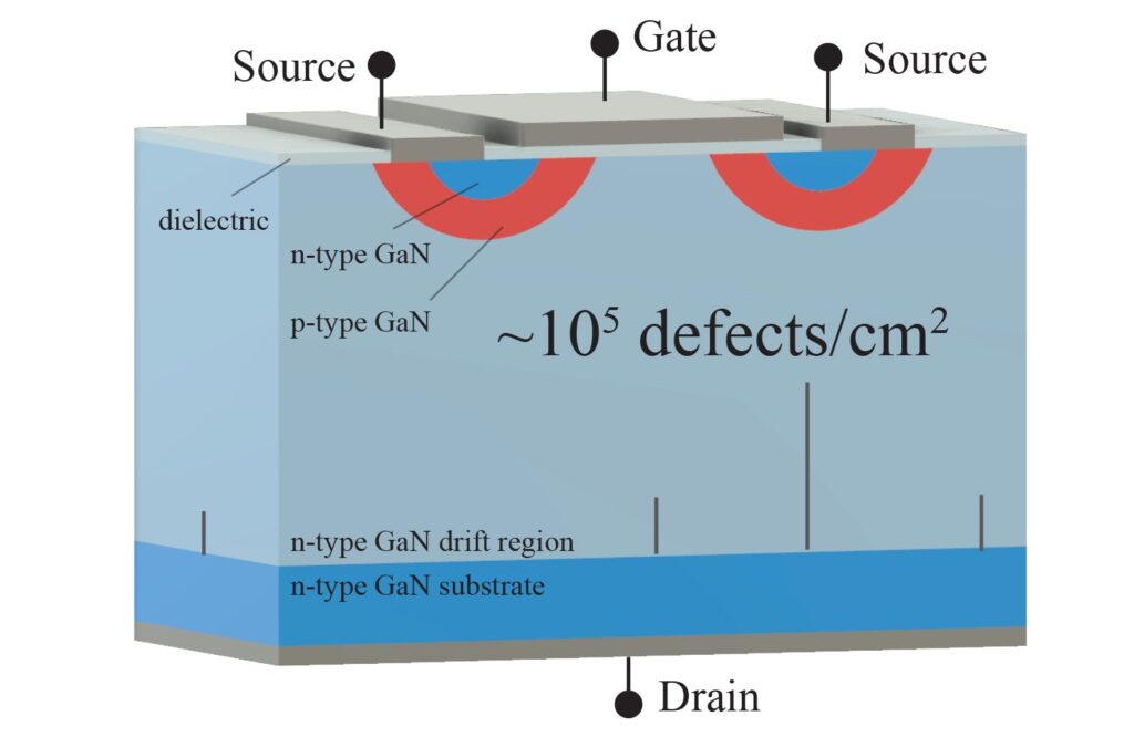
Currently, bulk GaN substrates are not available in sizes larger than 100mm, significantly increasing the costs of v-GaN devices. However, v-GaN devices have much smaller die sizes than SiC devices, helping to close the cost gap. The availability of larger bulk GaN substrates will be one key to bringing down the cost of v-GaN power transistors. Higher frequencies that enable the use of smaller and lower cost passives and the increased efficiencies anticipated for v-GaN power converters will also be keys in any future adoption of this emerging technology.
Summary
The superior performance of GaN HEMTs arises in part from material properties that include the widest energy gap, the largest critical field, and the highest saturation velocity of common semiconductor materials. Lateral GaN devices have no oxide dielectric in the gate structure or p-n drain to source junction. The GaN devices have very small parasitic capacitance and switching charges enabling very high-frequency operation. Many GaN solutions are available to designers, including discrete e-mode GaN transistors, d-mode high-voltage GaN devices in cascode structures with low-voltage Si MOSFETs, and a range of integrated GaN solutions that can simplify the design process and speed time to market. Most recently, v-GaN devices have appeared that promise to increase the operating voltages of GaN from today’s limit of 600 to 900 V up to 10 kV or more.
References
An Introduction to GaN Enhancement-mode HEMTs, GaN Systems
An Overview of Normally-Off GaN-Based High Electron Mobility Transistors, MDPI materials
Critical Transient Processes of Enhancement-mode GaN HEMTs in High-efficiency and High-reliability Applications, CES Transactions on Electrical Machines and Systems
Electrify Our World, Navitas Semiconductor
Enhance-Mode Gallium Nitride Technology, EPC
GaN-based power devices: Physics, reliability, and perspectives, Journal of Applied Physics
GaN Explained, Power Integrations
GaN FETs: Why cascode?, Nexperia
What is a wide-band-gap semiconductor?, Toshiba Electronic Devices and Storage
Why GaN Technology?, Odyssey Semi



Leave a Reply