
by Anup Bhalla, VP Engineering, UnitedSiC
Wide bandgap semiconductors are enablers for highly efficient power conversion. There is a choice of devices to use, including SiC FETs, a silicon and SiC technology hybrid. This article discusses the characteristics of the devices in comparison with other approaches.
High efficiency is the universal aim in the world of power conversion – it is an enabler for cost and energy savings, less environmental impact, smaller, lighter, more reliable equipment, and better functionality. This is no truer than in current and emerging applications; server farms, for example, are said to consume over 1 percent of global energy from heat dissipated from electronics and air conditioning [1]. In the application, end voltages at server blades can be sub-1V at current levels of hundreds of amps, making losses potentially heavier in interconnection resistances and semiconductor drops.
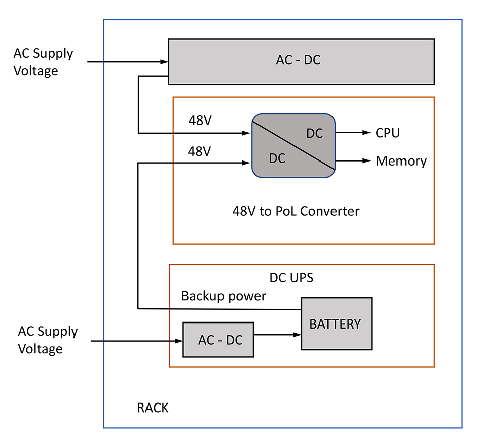
Data centers use power distribution schemes to maximize efficiency
Efforts by system architects to improve efficiency have paid off, with server farm energy draw increasing only around 6 percent from 2010 to 2018, despite internet traffic increasing 10x and data center storage expanding 20x in the same period [1]. This has been achieved by schemes of intermediate buses in the conversion from AC supply down to load voltage, with the ‘current trend towards an internal bus at around 385VDC, derived from an AC-DC power factor correction stage, then down-converted with isolation, to a bus at 48V with battery back-up, followed by isolated or non-isolated ‘point of load’ DC-DC converters (Figure 1).
The efficiency of the individual power conversion stages has dramatically improved as well, spurred on by standards such as ‘80+ Titanium’, which targets 96 percent efficiency at 50 percent load and 230VAC input. Novel topologies have enabled this, such as the ‘bridgeless totem-pole PFC’ stage and resonant DC-DC converters such as the phase-shifted full-bridge and ‘LLC’ converter, but semiconductor technology has advanced as well, particularly with the use of wide band-gap switches in silicon carbide (SiC) and gallium nitride (GaN).
EVs drive efficiency advances
It could be said that a modern EV is a mobile data center with a large helping of industrial-scale electrical motion control thrown in (Figure 2). As such, power conversion and motor control efficiency are key to the inherent viability of the mode of transport, with improvements driving a virtuous circle of smaller size and weight of converters and batteries for a longer range at a lower cost. The main lithium-ion battery ranges from 48V for mild hybrids to 400-800V for full-electric versions. In all cases, a traction inverter is needed, normally bi-directional, with various DC-DC converters for auxiliary services. In most cases, an onboard AC-DC charger is required, also often bi-directional, to return energy to the grid for cash credit. Wide band-gap semiconductors are again used for their low losses. The control electronics can facilitate forward and reverse energy flow when dynamically configured alternatively as switches or synchronous rectifiers.

There is some resistance to converting traction inverters from IGBT technology to SiC or GaN as the high-frequency capability of the wide band-gap devices is not of obvious value, with sub-20kHz switching still typical. IGBTs can be efficient at these frequencies, and they have a long record of durability at a low cost. However, the on-state losses and residual switching losses can now be significantly reduced with SiC, so the technology is increasingly adopted. IGBTs also require parallel diodes for motor drives and bi-directional capability, whereas SiC has an integral diode, though not necessarily high performance.
High-efficiency power conversion topologies
All power converters fall into two basic categories: ‘buck’ and ‘boost’ or equivalently ‘forward’ and ‘flyback’ in isolated formats. There is a minimum of one switch and one diode in all cases, and the most complex multi-level variants can have tens of semiconductors. For high efficiency, the diode is replaced by a ‘synchronous rectifier,’ a switch emulating a diode by active control of its gate. Now, semiconductor voltage drops and consequent conduction losses are defined only by device on-resistances and can be minimized by selecting the best affordable device.
Switching losses are harder to keep under control; faster edges generally result in less voltage and current overlap with its consequent transient dissipation, but losses increase proportionally with switching frequency, so if the limits of SiC or GaN are pushed to reduce the size, cost, and weight of magnetics, switching losses can still be substantial. For this reason, ‘soft’ or resonant switching is preferred in topologies where the current rise is delayed until the voltage has dropped to zero on switch-on (zero voltage switching or ZVS) or similarly zero current switching (ZCS) on turn off. Control ensures ZVS and ZCS can be complex, dependent on operating conditions, and converters designed for resonant operation can fall into lossy ‘hard’ switching under overload or transient input conditions. In practice, some conversion stages, such as the totem-pole PFC, must be operated in hard-switched ‘continuous conduction mode’ (CCM) at high power. The alternatives, discontinuous or critical conduction modes, produce unacceptably high peak and RMS currents in switches and magnetics.
An example of high-efficiency topology – the LLC converter
To illustrate design techniques for high efficiency, we can look at the LLC converter, so named because the primary consists of a resonant circuit of a capacitor and two inductors, one of which is the transformer primary winding (Figure 3).
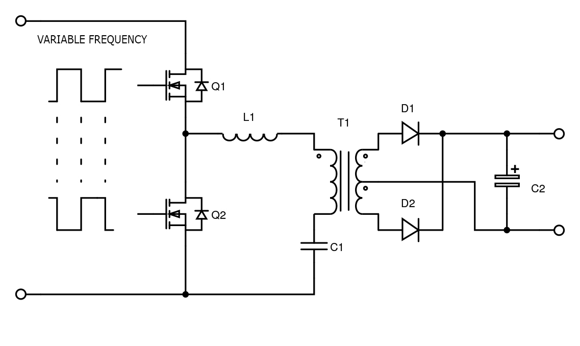
The two switches Q1 and Q2, operate similarly to a ‘buck’ converter but are simply driven with a constant, near-50 percent duty cycle, anti-phase signals with a controlled dead-time. This creates a square-wave drive to the resonant tank formed by L1 and T1 primary, and simplistically, impedance is minimum, and the output voltage is maximum when the square wave is at the resonant frequency of the tank. Driven above or below resonance, the impedance rises, and output is less. Therefore, by varying frequency, the output voltage can be regulated. In practice, the operation is set to be above resonance under normal conditions so that the tank ‘looks’ inductive, and zero-volage switching naturally occurs for both Q1 and Q2. Zero current switching in the output diode also naturally occurs. Control is quite complex, with multiple resonances occurring, also affected by load value.
Switch parasitics define effectiveness in high-efficiency topologies
Efficient resonant operation of circuits like the LLC is affected by the choice of semiconductors and their characteristics; output capacitance COSS and stored energy EOSS have to be discharged before switching, and the values are high and variable in Silicon MOSFETs, for example. The action of charging and discharging COSS also causes losses in itself. SiC MOSFETs typically have lower values, but in either case, in fabrication, MOSFETs have to trade off on-resistance with EOSS, so a useful comparative figure of merit is RDS(ON).EOSS . Another useful FOM is RDS(ON).A, the product of on-resistance and die area, which again trade-off with each other – smaller die to give better yield per wafer and cost-effectiveness, but with smaller channel areas giving higher on-resistance.
The reverse conduction characteristics are also important – SiC MOSFETs have a high forward voltage drop across their body diode, giving conduction losses during reverse conduction in ‘dead’ times. The drop is higher than with the older Si-MOSFET technology. SiC MOSFET reverse recovery energy is also present, although much better than typical Si-MOSFETs. GaN HEMT cells have very low reverse recovery as they simply conduct through their channel in reverse. Still, the voltage drop can be even higher than SiC MOSFETs if a negative off-state gate drive voltage is used, adding to the effective total voltage drop. Although an enhancement-mode GaN HEMT cell is nominally off with zero gate voltage, this negative drive is often recommended to avoid spurious turn on with the low threshold voltage. Common inductance to the source connection and gate drive loop is a typical cause of transient voltages with high drain di/dt that can cause the effect. Again, to characterize the effect of the channel and reverse conduction losses across switch types, the FOM RDS(ON). Qrr is useful.
Comparing the choice of switch technologies
A summary of device characteristics and FOMs that affect efficiency is given in Table 1 for two silicon superjunction MOSFETS, a SiC-MOSFET, a GaN HEMT cell, and an alternative we can now discuss, the SiC FET, all for the same voltage and drain current class of device.
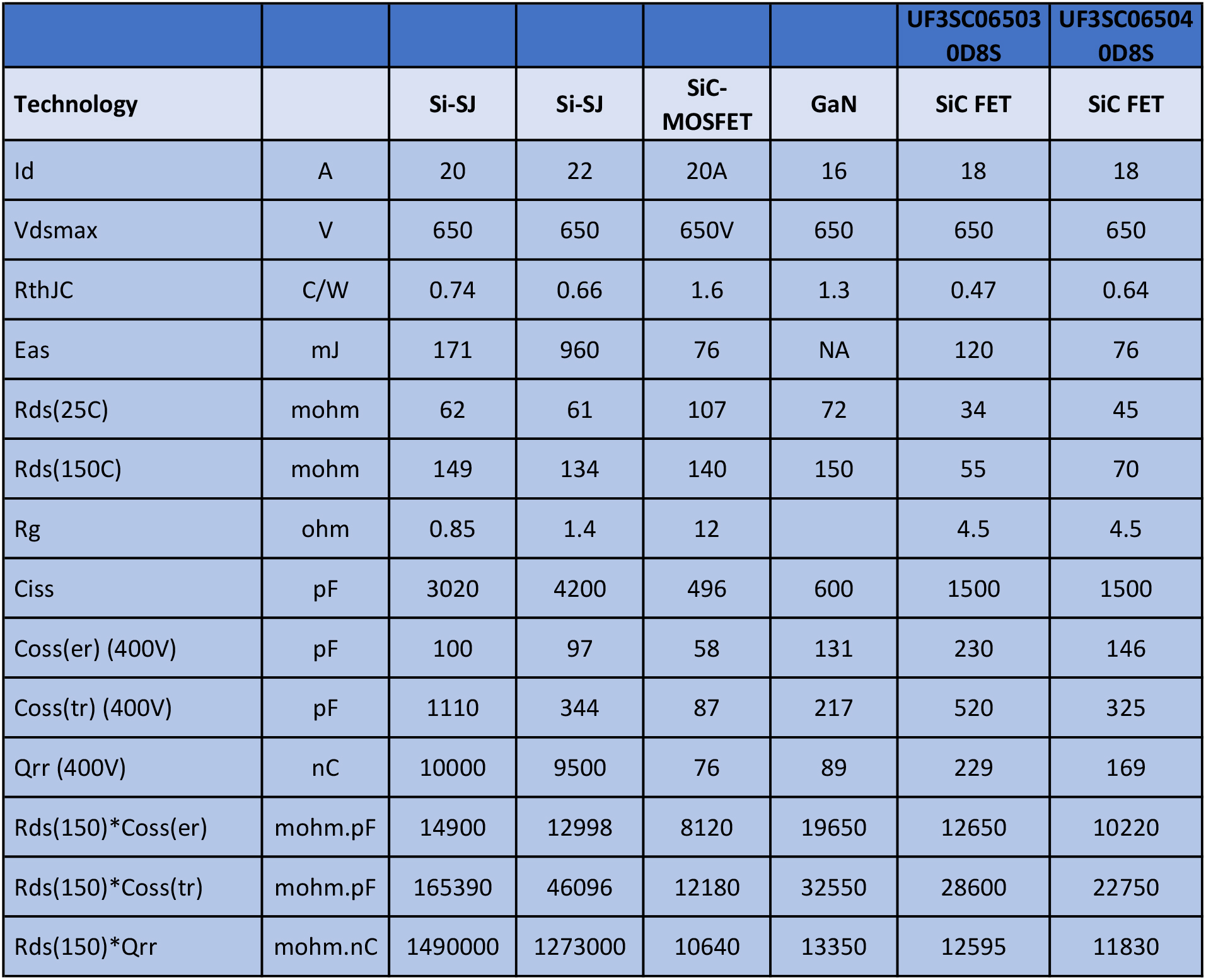
The table clearly shows the benefit of dynamic characteristics of SiC MOSFETs and GaN over silicon superjunction MOSFETs of a similar class. However, conduction losses are similar and thermal resistance to case and avalanche energy rating Eas is typically worse. However, SiC FETs are also shown as an alternative. SiC FETs are a cascode arrangement of a SiC JFET and a silicon MOSFET with substantially lower on-resistance. Their typically silver-sintered die-attach improved thermal resistance to the case compared to the others. Dynamic FOMs for SiC FETs are as good or better than the other technologies.
A major practical advantage of the SiC FET is the easy gate drive compared with SiC MOSFETs and GaN cells. SiC MOSFETs must be driven to around 18V at the gate for full enhancement, very close to the absolute maximum, 23V for the device shown. The gate threshold voltage is also variable and exhibits some hysteresis. E-GaN cells have a very low threshold voltage and an absolute maximum of only about 7V, so care must be taken to prevent stress from gate voltage transients or overshoots. SiC FETs, in comparison, have a robust gate with a threshold compatible with Si-MOSFETs or even IGBTs so they can be safely driven at 0-12V with an absolute maximum of a distant +/-25V for the devices described. If there is any problem applying SiC FETs, they are very fast, with the risk of EMI, overshoots, and ringing. Series resistance in the Si-MOSFET gate is not a good way to control this, as the SiC JFET gate is isolated in the cascode arrangement. However, it has been shown that smaller RC snubbers are an effective solution and a better trade-off in managing EMI while keeping losses at a minimum. This is especially true when switching off large currents in circuits with large parasitic inductances. It also simplifies parallel operation of fast switching devices.
There is a choice of wide band-gap devices that can be used for the highest efficiency in power converters, and in the past, the application very much drove the decision of which to use. SiC FETs available from UnitedSiC [2] can be used in all common topologies for a useful boost in performance.
References
1) https://energyinnovation.org/2020/03/17/how-much-energy-do-data-centers-really-use/


Leave a Reply