The design of an LLC resonant converter illustrates how eGaN FETs can shrink the physical size of modern supply circuitry.
Alex Lidow, Efficient Power Conversion Corp.
The rapid expansion of computing and telecommunications has brought a migration to a 48 V-based power architecture. Applications for this higher-voltage architecture include artificial intelligence, 5G, big data, and cloud servers demanding higher power density, higher power per board, and higher component density. Because real estate is extremely valuable on these high-density computing boards, there is a high premium on power density.
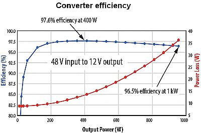
Consequently, there is a lot of interest in 48-to-12-V on-board dc-dc converters. The Distributed-power Open Standards Alliance (DOSA) sets size limits on 1/8th power brick-format 48-V server applications. In that regard, consider a 1-kW, 4:1-conversion ratio, eGaN FET-based LLC resonant converter. This converter hits 97.5% peak and 96.7% full-load efficiency. It can move beyond the limitations of the DOSA standard to realize even higher power density through use of GaN integration.
Typical specs in this application area are for a 1-kW load power-capable 48-to-12-V converter that operates in the range from 40 through 60 V. The converter design must fit in a volume defined by 58.4×22.9×10 mm, which is similar in size to a DOSA 1/8th-brick converter, with a maximum allowable airflow limited to 400 LFM. In addition, the final module had to be fitted with connection pins for either horizontal or vertical mounting. Finally, the input and output needs no isolation, which presents simplifies both the topology and design.
Design overview
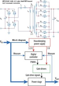
In this design, a full-bridge, primary-side configuration generates the pulsed input voltage to the resonant tank circuit. The tank is comprised of a resonant capacitor in series with a resonant inductor by using the transformer leakage inductance.
The design uses a high-frequency planar transformer with 4:1 turns ratio designed as a matrix transformer comprised of two series 2:1:1 connected sections wound around a single two-post core. The transformer magnetizing inductance in conjunction with a pre-determined dead time setting is used to establish zero-voltage switching (ZVS) on the primary-side FETs. Switches Q1/Q4 and Q2/Q3 switch at near 50% duty cycle and at 180° out-of-phase with each other. Two parallel center-tapped half-bridge arms are used in the secondary side, together with synchronous rectifier FETs for the output. This synchronous rectification scheme reduces the secondary side conduction losses at high-load currents.
eGaN FETs are well suited for soft-switching LLC resonant converters. Compared to silicon MOSFETs of similar ratings, their lower gate charge (QG) and 5-V gate operation brings much lower gate power consumption. In addition, GaN FETs have much lower output capacitance and thus need much less energy to realize ZVS. Lower output capacitance would either reduce the dead time and boost the effective power delivering time, or reduce the required magnetizing current, circulating energy and conduction losses. Finally, eGaN FETs are three to five times smaller than their aging MOSFET counterparts.
The design uses the 100-V, 3.2-mΩ EPC2218 and 40-V, 1.5-mΩ EPC2024 for the primary- and secondary-side power devices respectively. Both eGaN FETs can operate at up to 150°C junction temperature. The small form factor of GaN FETs make it possible to fit eight FETs in the limited 1/8th power brick size for the synchronous rectifiers.
The design also includes on-board housekeeping power supply, digital controller, and input and output voltage sensing. To command the power stage, a dsPIC controller (dsPIC33CK32MP102-I/2N) from Microchip generates high-resolution PWM signals. The on-board housekeeping power supply generates the 5 V needed for the gate drivers and the 3.3 V for the controller.
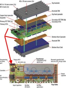
A combination of custom-shaped heat spreaders and a finned heatsink for the top and bottom side of the EPC9149 board were designed to be added to the 1-kW converter. Copper heat spreaders sit on top of both primary- and secondary-side FETs to spread their heat to the outer structure. The copper heat spreaders include contour features that allow parts of the heat spreader to rest on the PCB to facilitate cooling, mechanical stability and define the correct spacing between the heat spreader and the FET top surfaces.
A high-performance thermal interface material (TIM)–such as T-global A1780 with high thermal conductivity of 17.8 W/m-K–provides insulation and high thermal conductivity between the components and the metal surface of heat spreaders. A 2:1 compression ratio provides adequate force for best thermal performance, but not so much compression as to mechanically stress any components. TIM also provides isolation for grounding the heatsink. A second thermal interface material–TG-A6200, also from T-Global, which has a thermal conductivity of 6.2 W/m-K–interfaced the heat spreader to the heatsink. Mechanical screws on the board hold the entire mechanical structure in place.
The EPC9149 1-kW, 4:1 ratio GaN FET-based LLC resonant converter module was affixed to a motherboard for evaluation. The main input and output connections, measurement ports, bulk input and output capacitors, USB and communication port all sit on the motherboard. The low gate capacitance, output charge and on-resistance and the small form factor of the eGaN FETs are keys to high efficiency at a power density exceeding 1,227 W/in3.
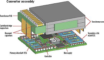
The EPC9149 is an example of the state-of-the-art for 48-to-12-V on-board dc-dc converters. There are ways to further improve power density. First, the long-and-thin aspect ratio of design was forgone for a squarer format that allowed significant improvement in the transformer design. The second improvement was driven by a 3D assembly approach where the transformer was separated from the power converter stage. This approach allowed improvement of both designs with fewer compromises.
The next improvement is to upgrade to the next generation of eGaN FETs. For the follow-on design, the 40-V, 1.5 mΩ device used on the EPC9149 is upgraded to a 40-V, 1 mΩ device. The combination of these improvements brings a power density of 5,130 W/in3 – a huge leap forward!
GaN integration
In 2014, EPC devised the first GaN integrated circuits, monolithic half bridges. The advantages of this integration included reductions in both size and cost and, by virtue of the close coupling of the two transistors, reduction of the parasitic common-source inductances.

In early 2019, the driver function and the monolithic half bridge were merged onto a single GaN-on-silicon substrate along with a level shifter, synchronous boost circuit, protection, and input logic. This complete EPC2152 ePower Stage can be driven at multi-megahertz frequencies and controlled by a simple low-side CMOS IC. With the addition of just a few passive components, it can become a complete dc-dc regulator. This regulator is 35% smaller and has half the components of a discrete implementation with a higher efficiency. In the next few years, there will be complete system-on-a-chip designs that include all the main functions required for a state-of-the-art dc-dc converter.
The impact of this integration on the 48–12-V on-board dc-dc converters will be dramatic. Implementing eGaN power stage ICs on the primary side and synchronous rectification ICs on the secondary side doubles the amount of area that can be used for the GaN circuits. This integration greatly reduces and will eventually eliminate housekeeping circuits and controllers. The estimate is that the losses due to GaN and the peripheral components can be halved to yield an additional 50% higher power density.
The trend toward higher power density is not abating. eGaN devices provide a way to realize the maximum power density possible today, and the next generation of devices and integrated solutions will take advances even further.
References
A. Lidow, editor, GaN Power Devices and Applications, 1st ed. Power Conversion Press, 2022. ISBN: 978-0-9966492-2-3
A. Lidow, M. de Rooij, J. Strydom, D. Reusch, J. Glaser, GaN Transistors for Efficient Power Conversion, 3rd ed., J. Wiley 2020. ISBN-13: 978-1119594147
Efficient Power Conversion Corp. (2021), EPC2218 datasheet, EPC2218 – 100 V, 231 A Enhancement-Mode GaN Power Transistor
Efficient Power Conversion Corp. (2021), EPC2024 datasheet, EPC2024 – 40 V, 90 A Enhancement-Mode Power Transistor
Microchip Technology Inc., dsPIC33CK32MP102-I/2N datasheet, 100 MHz Single-Core 16-Bit Digital Signal Controller
EPC9149 Efficient Power Conversion Corp. (2015), EPC9149 Quick Start Guide, EPC9149: 36 – 60 V Input, 9 – 15 V Output, 83 A Output Fixed Conversion Ratio 1 kW LLC, 1/8th Brick size Module Quick Start Guide
T-Global Technology, TG-A1780 datasheet, TG-A1780 Ultra soft thermal pad
T-Global Technology, TG-A6200 datasheet, TG-A6200 Ultra soft thermal pad
Efficient Power Conversion Corp. EPC2152 Datasheet, EPC2152 – 80 V, 15 A ePower™ Stage






Leave a Reply