
 GaN Systems announced a new reference design for the highest power density, high efficiency GaN-based 65W Active Clamp Flyback (ACF) charger in collaboration with Silanna Semiconductor. The reference design is now available at Silanna Semiconductor and provides an easy design for ACF USB-C PD GaN chargers, reducing design cycles and product time to market for customers.
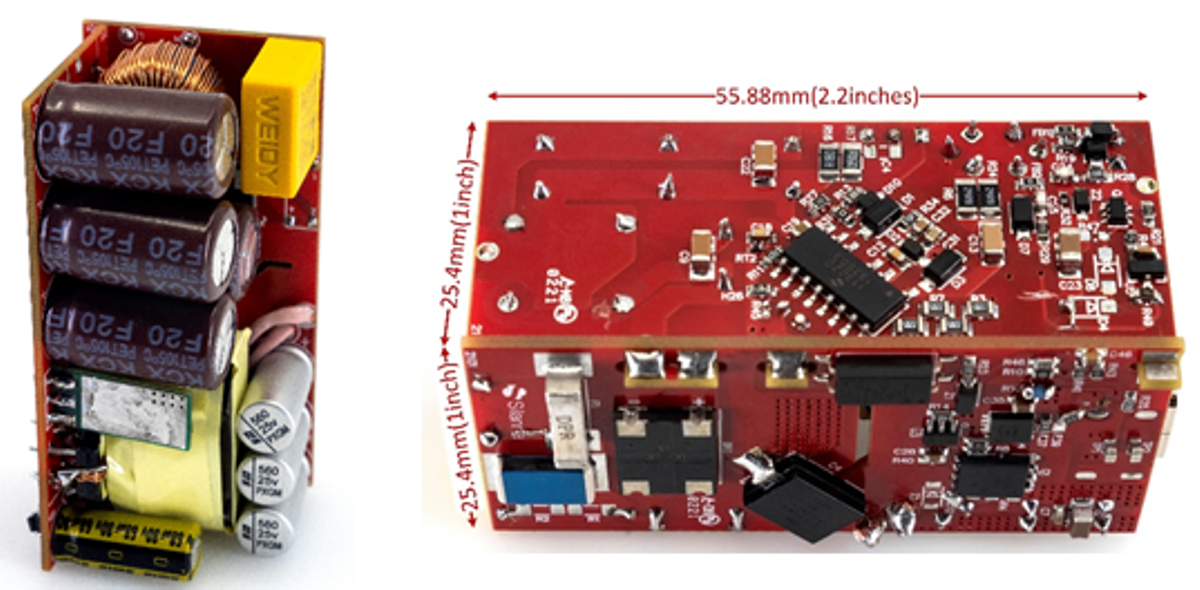
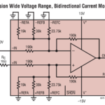
This solution removes the difficulties of an ACF topology design, which typically has two transistors in the high-side and in the low-side configuration. The new charger reference design uses Silanna Semiconductor’s SZ1130 ACF Pulse Width Modulator (PWM) controller and GaN Systems GS-065-008-1-L 650V GaN power transistor, with the high-side FET integrated into the controller. This design results in lower BoM costs by using a conventional RM8 transformer and 100V SR MOSFET on the secondary side.
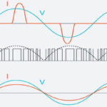
Key Benefits and Features include: Ultra-high density: 30W/in^3 no case; High efficiency: peak efficiency >94%; Low temperature: <95◦C max component temperature; Better EMI design: Clean waveforms with almost zero voltage spike or ringing; Supports a wide range of applications: 5V/3A, 9V/3A, 15V/3A, and 20V/3.25A output voltages; USB-PD


Leave a Reply